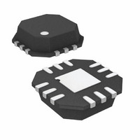
ADG1236YCPZ-500RL7 Analog Devices Inc, ADG1236YCPZ-500RL7 Datasheet - Page 8

ADG1236YCPZ-500RL7
Manufacturer Part Number
ADG1236YCPZ-500RL7
Description
IC,ANALOG SWITCH,DUAL,SPDT,CMOS,LLCC,12PIN,PLASTIC
Manufacturer
Analog Devices Inc
Series
iCMOS®r
Type
Analog Switchr
Datasheet
1.ADG1236YCPZ-500RL7.pdf
(16 pages)
Specifications of ADG1236YCPZ-500RL7
Function
Switch
Circuit
2 x SPDT
On-state Resistance
260 Ohm
Voltage Supply Source
Single Supply
Voltage - Supply, Single/dual (±)
12V, 15V
Current - Supply
1µA
Operating Temperature
-40°C ~ 125°C
Mounting Type
Surface Mount
Package / Case
12-VFQFN, CSP Exposed Pad
Multiplexer Configuration
Dual SPDT
Number Of Inputs
2
Number Of Outputs
4
Number Of Channels
2
Analog Switch On Resistance
475@10.8VOhm
Analog Switch Turn On Time
150ns
Analog Switch Turn Off Time
190ns
Package Type
LFCSP
Power Supply Requirement
Single/Dual
Single Supply Voltage (typ)
12V
Dual Supply Voltage (typ)
±15V
Power Dissipation
3.5mW
Supply Current
0.23mA
Mounting
Surface Mount
Pin Count
12
Operating Temp Range
-40C to 125C
Operating Temperature Classification
Automotive
Lead Free Status / RoHS Status
Lead free / RoHS Compliant
Lead Free Status / RoHS Status
Lead free / RoHS Compliant
Other names
ADG1236YCPZ-500RL7TR
ADG1236
TERMINOLOGY
I
The positive supply current.
I
The negative supply current.
V
The analog voltage on Terminals D and S.
R
The ohmic resistance between D and S.
R
Flatness is defined as the difference between the maximum and
minimum value of on resistance as measured over the specified
analog signal range.
I
The source leakage current with the switch off.
I
The drain leakage current with the switch off.
I
The channel leakage current with the switch on.
V
The maximum input voltage for Logic 0.
V
The minimum input voltage for Logic 1.
I
The input current of the digital input.
C
The off switch source capacitance, measured with reference to
ground.
DD
SS
S
D
D
INL
ON
FLAT(ON)
S
D
INL
INH
, I
(Off)
(Off)
(Off)
(V
(I
S
(On)
INH
S
)
)
Rev. 0 | Page 8 of 16
C
The off switch drain capacitance, measured with reference to
ground.
C
The on switch capacitance, measured with reference to ground.
C
The digital input capacitance.
t
The delay time between the 50% and 90% points of the digital
input and switch on condition when switching from one
address state to another.
Charge Injection
A measure of the glitch impulse transferred from the digital
input to the analog output during switching.
Off Isolation
A measure of unwanted signal coupling through an off switch.
Crosstalk
A measure of unwanted signal that is coupled through from one
channel to another as a result of parasitic capacitance.
Bandwidth
The frequency at which the output is attenuated by 3 dB.
On Response
The frequency response of the on switch.
Insertion Loss
The loss due to the on resistance of the switch.
THD + N
The ratio of the harmonic amplitude plus noise of the signal to
the fundamental.
TRANS
D
D
IN
, C
(Off)
S
(On)


