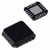
ADF4001BCPZ-RL7 Analog Devices Inc, ADF4001BCPZ-RL7 Datasheet - Page 7

ADF4001BCPZ-RL7
Manufacturer Part Number
ADF4001BCPZ-RL7
Description
Clock Generation PLL
Manufacturer
Analog Devices Inc
Type
Clock Generator (RF)r
Datasheet
1.ADF4001BRUZ.pdf
(16 pages)
Specifications of ADF4001BCPZ-RL7
Pll
Yes
Input
Clock
Output
Clock
Number Of Circuits
1
Ratio - Input:output
2:1
Differential - Input:output
Yes/No
Frequency - Max
200MHz
Divider/multiplier
Yes/No
Voltage - Supply
2.7 V ~ 5.5 V
Operating Temperature
-40°C ~ 85°C
Mounting Type
Surface Mount
Package / Case
20-LFCSP
Frequency-max
200MHz
Lead Free Status / RoHS Status
Lead free / RoHS Compliant
For Use With
EVAL-ADF4001EBZ2 - BOARD EVAL FOR ADF4001
Lead Free Status / RoHS Status
Lead free / RoHS Compliant
Lock Detect
MUXOUT can be programmed for two types of lock detect:
digital lock detect and analog lock detect. Digital lock detect is
active high. When LDP in the R counter latch is set to 0, digital
lock detect is set high when the phase error on three consecutive
phase detector cycles is less than 15 ns. With LDP set to 1, five
consecutive cycles of less than 15 ns are required to set the lock
detect. It will stay set high until a phase error of greater than
REV. A
ANALOG LOCK DETECT
DIGITAL LOCK DETECT
DB23
DB23
DB23
DB23
X = DON’T CARE
RESERVED
RESERVED
R COUNTER OUTPUT
N COUNTER OUTPUT
RESERVED
X
X
X
X
RESERVED
DB22
DB22
DB22
DB22
X
X
X
X
DB21
GAIN
DB21
DB21
DB21
G1
PD2
PD2
SDOUT
CP
X
Figure 6. MUXOUT Circuit
DB20
DB20
DB20
DB20
N13
CPI6
CPI6
LDP
CURRENT
CURRENT
SETTING
SETTING
DB19
DB19
DB19
DB19
N12
CPI5
CPI5
T2
2
2
MODE
TEST
MUX
BITS
DB18
DB18
DB18
DB18
T1
N11
CPI4
CPI4
DB17
ABP2
DB17
DB17
DB17
N10
CPI3
CPI3
BACKLASH
WIDTH
ANTI-
CURRENT
CURRENT
SETTING
SETTING
CONTROL
DB16
DB16
DB16
DB16
ABP1
N9
CPI2
CPI2
1
1
Table II. ADF4001 Family Latch Summary
DB15 DB14
DB15 DB14
DB15 DB14
DB15 DB14
R14
N8
CPI1
CPI1
13-BIT N COUNTER
REFERENCE COUNTER LATCH
DGND
DV
R13
N7
TC4
TC4
DD
INITIALIZATION LATCH
N COUNTER LATCH
MUXOUT
TIMER COUNTER
TIMER COUNTER
FUNCTION LATCH
DB13
DB13
DB13
DB13
R12
N6
TC3
TC3
CONTROL
CONTROL
DB12
DB12
DB12
DB12
R11
N5
TC2
TC2
–7–
DB11
DB11
DB11
DB11
25 ns is detected on any subsequent PD cycle. The N-channel
open-drain analog lock detect should be operated with an external
pull-up resistor of 10 kΩ nominal. When lock has been detected,
this output will be high with narrow low-going pulses.
INPUT SHIFT REGISTER
The ADF4001 digital section includes a 24-bit input shift regis-
ter, a 14-bit R counter, and a 13-bit N counter. Data is clocked
into the 24-bit shift register on each rising edge of CLK. The
data is clocked in MSB first. Data is transferred from the shift
register to one of four latches on the rising edge of LE. The
destination latch is determined by the state of the two control
bits (C2, C1) in the shift register. These are the two LSBs, DB1
and DB0, as shown in the timing diagram of Figure 1. The truth
table for these bits is shown in Table I. Table II shows a sum-
mary of how the latches are programmed.
R10
N4
TC1
TC1
14-BIT REFERENCE COUNTER
DB10
DB10
DB10
DB10
R9
N3
F5
F5
C2
0
0
1
1
DB9
DB9
DB9
DB9
R8
N2
F4
F4
Control Bits
DB8
DB8
DB8
DB8
Table I. C2, C1 Truth Table
R7
N1
F3
F3
C1
0
1
0
1
DB7
DB7
DB7
DB7
R6
F2
F2
X
DB6
DB6
DB6
DB6
R5
M3
M3
X
CONTROL
CONTROL
MUXOUT
MUXOUT
DB5
DB5
DB5
DB5
RESERVED
R4
M2
M2
X
Data Latch
R Counter
N Counter
Function Latch
Initialization Latch
DB4
DB4
DB4
DB4
R3
M1
M1
X
DB3
DB3
R2
DB3
PD1
DB3
PD1
X
ADF4001
DB2
DB2
DB2
DB2
R1
F1
F1
X
C2 (0) C1 (0)
C2 (0) C1 (1)
C2 (1) C1 (0)
C2 (1) C1 (1)
DB1
DB1
DB1
DB1
CONTROL
CONTROL
CONTROL
CONTROL
BITS
BITS
BITS
BITS
DB0
DB0
DB0
DB0


