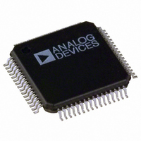
ADAV803ASTZ-REEL Analog Devices Inc, ADAV803ASTZ-REEL Datasheet - Page 28

ADAV803ASTZ-REEL
Manufacturer Part Number
ADAV803ASTZ-REEL
Description
IC,Soundcard Circuits,QFP,64PIN,PLASTIC
Manufacturer
Analog Devices Inc
Type
Audio Codecr
Datasheet
1.ADAV803ASTZ-REEL.pdf
(60 pages)
Specifications of ADAV803ASTZ-REEL
Data Interface
Serial
Resolution (bits)
24 b
Number Of Adcs / Dacs
2 / 2
Sigma Delta
No
Dynamic Range, Adcs / Dacs (db) Typ
102 / 101
Voltage - Supply, Analog
3 V ~ 3.6 V
Voltage - Supply, Digital
3 V ~ 3.6 V
Operating Temperature
-40°C ~ 85°C
Mounting Type
Surface Mount
Package / Case
64-LQFP
Lead Free Status / RoHS Status
Lead free / RoHS Compliant
For Use With
EVAL-ADAV803EBZ - BOARD EVALUATION FOR ADAV803
Lead Free Status / RoHS Status
Lead free / RoHS Compliant
Available stocks
Company
Part Number
Manufacturer
Quantity
Price
Company:
Part Number:
ADAV803ASTZ-REEL
Manufacturer:
Analog Devices Inc
Quantity:
10 000
ADAV803
DIR PLL(512 ×
DIR PLL(256 ×
DIR PLL(512 ×
DIR PLL(256 ×
LRCLK
LRCLK
LRCLK
SDATA
SDATA
SDATA
BCLK
BCLK
BCLK
PLLINT1
PLLINT2
PLLINT1
PLLINT2
PLLINT1
PLLINT2
PLLINT1
PLLINT2
MCLKI
MCLKI
MCLKI
MCLKI
XIN
XIN
XIN
XIN
f
f
f
f
S
S
S
S
REG 0x76
REG 0x76
REG 0x77
REG 0x76
BITS[4:2]
)
)
BITS[7:5]
)
)
BITS[4:3]
BITS[1:0]
Figure 50. SPORT Clocking Scheme
MSB
DIR PLL(512 ×
DIR PLL(256 ×
REG 0x00
BITS[3:2]
REG 0x00
BITS[4:5]
MSB
DIVIDER
DIVIDER
PLL CLOCK
PLL CLOCK
MCLK
MCLK
ADC
DAC
ICLK1
ICLK2
ICLK1
ICLK2
REG 0x00
BITS[1:0]
MSB
ICLK1
ICLK2
f
f
S
S
)
)
LEFT CHANNEL
LEFT CHANNEL
LEFT CHANNEL
OUTPUT
INPUT
PORT
PORT
REG 0x06
BITS[5:4]
REG 0x04
BITS[4:3]
MCLK
REG 0x00
BITS[7:6]
DIVIDER
RIGHT-JUSTIFIED MODE — SELECT NUMBER OF BITS PER CHANNEL
SRC
LEFT-JUSTIFIED MODE — 16 BITS TO 24 BITS PER CHANNEL
LSB
I
2
S MODE — 16 BITS TO 24 BITS PER CHANNEL
OLRCLK
OBCLK
OSDATA
ILRCLK
IBCLK
ISDATA
LSB
Figure 51. Serial Data Modes
Rev. A | Page 28 of 60
LSB
MSB
Care should be taken to ensure that the clock rate is appropriate
for whatever block is connected to the serial port. For example,
if the ADC is running from the MCLKI input at 256 × f
the master clock for the SPORT should also run from the
MCLKI input to ensure that the ADC and serial port are
synchronized.
The SPORTs can be set to transmit or receive data in I
justified or right-justified formats with different word lengths
by programming the appropriate bits in the playback register,
auxiliary input port register, record register, and auxiliary
output port-control register. Figure 51 is a timing diagram of
the serial data port formats.
Clocking Scheme
The ADAV803 provides a flexible choice of on-chip and off-
chip clocking sources. The on-chip oscillator with dual PLLs is
intended to offer complete system clocking requirements for
use with available MPEG encoders, decoders, or a combination
of codecs. The oscillator function is designed for generation of a
27 MHz video clock from a 27 MHz crystal connected between
the XIN and XOUT pins. Capacitors must also be connected
between these pins and DGND, as shown in Figure 35. The
capacitor values should be specified by the crystal manufacturer.
A square wave version of the crystal clock is output on the
MCLKO pin. If the system has a 27 MHz clock available, this
clock can be connected directly to the XIN pin.
MSB
MSB
RIGHT CHANNEL
RIGHT CHANNEL
RIGHT CHANNEL
LSB
LSB
LSB
2
S, left-
S
, then


