ADADC85-12 Analog Devices Inc, ADADC85-12 Datasheet
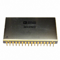
IC,A/D CONVERTER,SINGLE,12-BIT,HYBRID,DIP,32PIN

ADADC85-12

Manufacturer Part Number
ADADC85-12
Description
IC,A/D CONVERTER,SINGLE,12-BIT,HYBRID,DIP,32PIN
Manufacturer
Analog Devices Inc
Datasheet

Specifications of ADADC85-12

Rohs Status
RoHS non-compliant
Number Of Bits
12
Sampling Rate (per Second)
100k
Data Interface
Parallel
Number Of Converters
1
Voltage Supply Source
Dual ±
Operating Temperature
-55°C ~ 125°C
Mounting Type
Through Hole
Package / Case
32-CDIP (0.900", 22.86mm)
Lead Free Status / RoHS Status

Available stocks

Company
Part Number
Manufacturer
Quantity
Price
Part Number:
ADADC85-12
Manufacturer:
a
Quantity:
11
Part Number:
ADADC85-12
Manufacturer:
ADI
Quantity:
184
FEATURES
PERFORMANCE
Complete 12-bit A/D converter with reference and clock
Fast successive approximation conversion: 10 µs or 5 µs
Buried Zener reference for long-term stability and low
Max nonlinearity: < ±0.012%
Low power: 880 mW typ
Low chip count—high reliability
Industry-standard pinout
Z models for ±12 V operation available
MIL-STD-883B processing available
VERSATILITY
Negative true parallel logic outputs
Short cycle capability
Precision +6.3 V reference for external applications
PRODUCT DESCRIPTION
The AD ADC84/AD ADC85 series devices are high speed, low cost
12-bit successive approximation analog-to-digital converters that
include an internal clock, reference, and comparator. Its hybrid IC
design utilizes MSI digital and linear monolithic chips in
conjunction with a 12-bit monolithic DAC to provide modular
performance and versatility with IC size, price, and reliability.
Important performance characteristics of the AD ADC84/
AD ADC85 series include maximum linearity error of ±0.012%;
gain TC below 15 ppm/°C at 25°C; typical power dissipation of
880 mW; and conversion time of less than 10 µs for the 12-bit
versions. Of considerable significance in severe and aerospace
applications is the guaranteed performance from –55°C to +125°C
of the AD ADC85S, which is also available with environmental
screening. Monotonic operation of the feedback DAC guarantees
no missing codes over temperature ranges of 0°C to +70°C, –25°C
to +85°C, and –55°C to +125°C.
The design of the AD ADC84/AD ADC85 includes scaling resistors
that provide analog input signal ranges of ±2.5 V, ±5 V, ±10 V, 0 V to
+5 V, or 0 V to +10 V. The 6.3 V precision reference, which can be
used for external applications, and the input buffer amplifier add
flexibility and value. All digital signals are fully DTL and TTL
compatible, and the data output is negative-true and available in
parallel form.
The AD ADC84/AD ADC85 are available in a performance grade
specified for 12-bit accuracy (±0.012% FSR max) with 10 µs
maximum conversion time.
Rev. B
Information furnished by Analog Devices is believed to be accurate and reliable.
However, no responsibility is assumed by Analog Devices for its use, nor for any
infringements of patents or other rights of third parties that may result from its use.
Specifications subject to change without notice. No license is granted by implication
or otherwise under any patent or patent rights of Analog Devices. Trademarks and
registered trademarks are the property of their respective owners.
Gain TC: 10 ppm/°C
The AD ADC84 and AD ADC85C are specified for operation over
the 0°C to +70°C temperature range. The AD ADC85 and
AD ADC85S are specified for the –25°C to +85°C and –55°C to
+125°C ranges, respectively. The serial output function is no longer
supported on the AD ADC84/AD ADC85 after date code 9623.
PRODUCT HIGHLIGHTS
1.
2.
3.
4.
5.
6.
7.
One Technology Way, P.O. Box 9106, Norwood, MA 02062-9106, U.S.A.
Tel: 781.329.4700
Fax: 781.326.8703
The AD ADC84/ AD ADC85 series devices are complete
12-bit ADCs. No external components are required to perform
a conversion.
The AD ADC84/ AD ADC85 directly replaces other devices of
this type with significant increases in performance.
The fast conversion rates of the AD ADC84 and AD ADC85
(10 μs) make them an excellent choice for applications
requiring high system throughput rates.
The internal buried Zener reference is laser trimmed to 6.3 V
±0.1% and ±10 ppm/°C typical TC. The reference is available
externally and can provide up to 1 mA.
The integrated package construction provides high quality and
reliability with small size and weight.
The monolithic 12-bit feedback DAC is used for reduced chip
count and higher reliability.
The AD ADC85S/883B comes processed to MIL-STD-883,
Class B requirements.
Figure 1. Functional Block Diagram
12-Bit A/D Converters
© 2003 Analog Devices, Inc. All rights reserved.
AD ADC84/AD ADC85
Fast, Complete
www.analog.com

Related parts for ADADC85-12

ADADC85-12 Summary of contents

Page 1

FEATURES PERFORMANCE Complete 12-bit A/D converter with reference and clock Fast successive approximation conversion: 10 µ µs Buried Zener reference for long-term stability and low Gain TC: 10 ppm/°C Max nonlinearity: < ±0.012% Low power: 880 mW typ ...

Page 2

AD ADC84/AD ADC85 TABLE OF CONTENTS Specifications..................................................................................... 3 Typical Performance Characteristics ............................................. 5 Functional Description .................................................................... 6 Offset Adjustment ........................................................................ 6 Gain Adjustment........................................................................... 6 Theory of Operation .................................................................... 6 Timing............................................................................................ 6 Digital Output Data ..................................................................... 7 REVISION HISTORY Revision B ...

Page 3

SPECIFICATIONS Table 1. Typical @ 25°C, ±15 V and +5 V, unless otherwise noted Model RESOLUTION ANALOG INPUTS Voltage Ranges Bipolar Unipolar Impedance (Direct Input ±2 +10 V, ±5 V ±10 ...

Page 4

AD ADC84/AD ADC85 Model DIGITAL OUTPUT (All Codes Complementary) Parallel Output Codes 7 Unipolar Bipolar Output Drive Status Status Output Drive Internal Clock Clock Output Drive Frequency INTERNAL REFERENCE VOLTAGE Maximum External Current (with No Degradation of Specifications) Tempco of ...

Page 5

TYPICAL PERFORMANCE CHARACTERISTICS Figure 2. Linearity Error vs. Conversion Speed Figure 3. Gain Drift Error (%FSR) vs. Temperature Figure 4. Change in Differential Linearity vs. Conversion Speed Figure 5. Conversion Speed vs. Control Voltage Rev Page 5 of ...

Page 6

AD ADC84/AD ADC85 FUNCTIONAL DESCRIPTION OFFSET ADJUSTMENT The zero adjust circuit consists of a potentiometer connected across ±V with its slider connected through a 1.8 MΩ resistor S to Comparator Input Pin 22 for all ranges. As shown in Figure ...

Page 7

NOTES 1. THE CONVERT START PULSE WIDTH IS 100ns MIN AND MUST REMAIN LOW DURING A CONVERSION. THE CONVERSION IS INITIATED BY THE “TRAILING EDGE” OF THE CONVERT COMMAND. 2. 10μs FOR 12 BITS (AD ADC84/AD ADC85). 3. MSB DECISION. ...

Page 8

AD ADC84/AD ADC85 INPUT SCALING The AD ADC84/AD ADC85 inputs should be scaled as close to the maximum input signal range as possible in order to utilize the maximum signal resolution of the A/D converter. Connect the input signal as ...

Page 9

CALIBRATION External ZERO ADJ and GAIN ADJ potentiometers, connected as shown in Figure 12 and Figure 13, are used for device calibration. To prevent interaction of these two adjustments, zero is always adjusted first and then gain. Zero is adjusted ...

Page 10

AD ADC84/AD ADC85 CLOCK RATE CONTROL ALTERNATE CONNECTIONS If adjustment of the CLOCK RATE is desired for faster conver- sion speeds, the CLOCK RATE CONTROL may be connected to an external multiturn trim potentiometer with a TCR of ±100 ppm/°C ...

Page 11

... ORDERING GUIDE 1 Model Operation Voltage (V) 2 ADADC84-12 ±15 2 ADADC84Z-12 ±12 ADADC85C-12 2 ±15 ADADC85-12 ±15 2 ADADC85Z-12 ±12 ADADC85S-12 ±15 ADADC85SZ-12 ±12 ADADC85S12/883B ±15 ADADC85SZ12/883 ±12 1 For complete model number, suffixes must be added for “Z” option (±12 V operation), linearity. The following guide shows the proper suffix order: AD ADC(*)(**)-(***), where * = Model Number Version Designator, and *** = Linearity ...

Page 12

AD ADC84/AD ADC85 NOTES © 2003 Analog Devices, Inc. All rights reserved. Trademarks and registered trademarks are the property of their respective owners. C03262–0–11/03(B) Rev Page ...

Related keywords