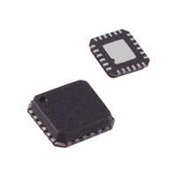
ADA4950-2YCPZ-RL Analog Devices Inc, ADA4950-2YCPZ-RL Datasheet - Page 23

ADA4950-2YCPZ-RL
Manufacturer Part Number
ADA4950-2YCPZ-RL
Description
Fixed Gain 1,2&3 Diff ADC Driver
Manufacturer
Analog Devices Inc
Datasheet
1.ADA4950-1YCPZ-R7.pdf
(28 pages)
Specifications of ADA4950-2YCPZ-RL
Amplifier Type
Differential
Number Of Circuits
2
Output Type
Differential
Slew Rate
2900 V/µs
-3db Bandwidth
750MHz
Voltage - Input Offset
200µV
Current - Supply
9.5mA
Current - Output / Channel
114mA
Voltage - Supply, Single/dual (±)
3 V ~ 11 V, ±1.5 V ~ 5.5 V
Operating Temperature
-40°C ~ 105°C
Mounting Type
Surface Mount
Package / Case
24-LFCSP
Lead Free Status / RoHS Status
Lead free / RoHS Compliant
Gain Bandwidth Product
-
Current - Input Bias
-
Lead Free Status / RoHS Status
Lead free / RoHS Compliant
LAYOUT, GROUNDING, AND BYPASSING
As a high speed device, the ADA4950-x is sensitive to the
PCB environment in which it operates. Realizing its superior
performance requires attention to the details of high speed
PCB design.
The first requirement is a solid ground plane that covers as
much of the board area around the ADA4950-x as possible. The
thermal resistance, θ
exposed pad, soldered to a high thermal conductivity 4-layer
circuit board, as described in EIA/JESD51-7.
Bypass the power supply pins as close to the device as possible
and directly to a nearby ground plane. Use high frequency
ceramic chip capacitors. It is recommended that two parallel
bypass capacitors (1000 pF and 0.1 μF) be used for each supply.
Place the 1000 pF capacitor closer to the device. Farther away,
provide low frequency bulk bypassing using 10 μF tantalum
capacitors from each supply to ground.
Figure 62. Cross-Section of 4-Layer PCB Showing Thermal Via Connection to Buried Ground Plane (Dimensions in Millimeters)
JA
, is specified for the device, including the
GROUND PLANE
BOTTOM METAL
POWER PLANE
TOP METAL
Rev. 0 | Page 23 of 28
VIA HOLE
PLATED
1.30
0.30
Signal routing should be short and direct to avoid parasitic
effects. Wherever complementary signals exist, provide a
symmetrical layout to maximize balanced performance. When
routing differential signals over a long distance, keep PCB
traces close together, and twist any differential wiring to
minimize loop area. Doing this reduces radiated energy and
makes the circuit less susceptible to interference.
Figure 61. Recommended PCB Thermal Attach Pad (Dimensions in Millimeters)
1.30
0.80
ADA4950-1/ADA4950-2
1.30
0.80


