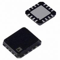
ADA4950-1YCPZ-R2 Analog Devices Inc, ADA4950-1YCPZ-R2 Datasheet - Page 3

ADA4950-1YCPZ-R2
Manufacturer Part Number
ADA4950-1YCPZ-R2
Description
Fixed Gain 1,2&3 Diff ADC Driver
Manufacturer
Analog Devices Inc
Type
Differential Amplifierr
Datasheet
1.ADA4950-1YCPZ-R7.pdf
(28 pages)
Specifications of ADA4950-1YCPZ-R2
Amplifier Type
Differential
Number Of Circuits
1
Output Type
Differential
Slew Rate
2900 V/µs
-3db Bandwidth
750MHz
Voltage - Input Offset
200µV
Current - Supply
9.5mA
Current - Output / Channel
114mA
Voltage - Supply, Single/dual (±)
3 V ~ 11 V, ±1.5 V ~ 5.5 V
Operating Temperature
-40°C ~ 105°C
Mounting Type
Surface Mount
Package / Case
16-LFCSP
No. Of Amplifiers
1
Input Offset Voltage
2.5mV
Bandwidth
750MHz
Supply Voltage Range
3V To 11V
Supply Current
9.5mA
Amplifier Case Style
LFCSP
No. Of Pins
16
Rohs Compliant
Yes
Number Of Channels
1
Number Of Elements
1
Power Supply Requirement
Single/Dual
Common Mode Rejection Ratio
49dB
Voltage Gain Db
66dB
Single Supply Voltage (typ)
5/9V
Dual Supply Voltage (typ)
±3/±5V
Power Supply Rejection Ratio
84dB
Rail/rail I/o Type
No
Single Supply Voltage (min)
3V
Single Supply Voltage (max)
11V
Dual Supply Voltage (min)
±1.5V
Dual Supply Voltage (max)
±5.5V
Operating Temp Range
-40C to 105C
Operating Temperature Classification
Industrial
Mounting
Surface Mount
Pin Count
16
Package Type
LFCSP EP
Lead Free Status / RoHS Status
Lead free / RoHS Compliant
Gain Bandwidth Product
-
Current - Input Bias
-
Lead Free Status / Rohs Status
Compliant
SPECIFICATIONS
±5 V OPERATION
T
refer to single-ended input and differential outputs, unless otherwise noted. Refer to Figure 52 for signal definitions.
Differential Inputs to V
Table 1.
Parameter
DYNAMIC PERFORMANCE
NOISE/HARMONIC PERFORMANCE
INPUT CHARACTERISTICS
OUTPUT CHARACTERISTICS
A
−3 dB Small-Signal Bandwidth
−3 dB Large-Signal Bandwidth
Bandwidth for 0.1 dB Flatness
Slew Rate
Settling Time to 0.1%
Overdrive Recovery Time
Second Harmonic
Third Harmonic
IMD3
Voltage Noise (Referred to Output)
Crosstalk (ADA4950-2)
Offset Voltage (Referred to Input)
Input Capacitance
Input Common-Mode Voltage Range
CMRR
Open-Loop Gain
Output Voltage Swing
Linear Output Current
Output Balance Error
Gain Error
= 25°C, +V
ADA4950-1
ADA4950-2
S
= 5 V, −V
S
OUT, dm
= −5 V, V
Performance
OCM
= 0 V, G = 1, R
Test Conditions/Comments
V
V
V
V
V
V
See Figure 51 for distortion test circuit
V
1 MHz
10 MHz
20 MHz
50 MHz
V
1 MHz
10 MHz
20 MHz
50 MHz
f
f = 1 MHz
Gain = 1
Gain = 2
Gain = 3
f = 10 MHz; Channel 2 active, Channel 1
output
V
T
Single-ended at package pin
Directly at internal amplifier inputs, not
external input terminals
DC, ∆V
Maximum ∆V
R
200 kHz, R
∆V
see Figure 50 for output balance test circuit
Gain = 1
Gain = 2
Gain = 3
1
MIN
OUT, dm
OUT, dm
OUT, dm
OUT, dm
OUT, dm
IN
OUT, dm
OUT, dm
+DIN
L
= 30 MHz, f
= 1 kΩ
OUT, cm
= 0 V to 5 V ramp, G = 2
to T
= V
OUT, dm
= 0.1 V p-p
= 2.0 V p-p
= 2.0 V p-p, R
= 2 V p-p, 25% to 75%
= 2 V step
= 2 V p-p
= 2 V p-p
/∆V
MAX
−DIN
L, dm
variation
OUT, dm
= V
/∆V
T
2
OUT
= 10 Ω, SFDR = 69 dB
= 53.6 Ω (when used), R
= 30.1 MHz, V
OCM
IN, cm
, single-ended output,
, ∆V
= 0 V
Rev. 0 | Page 3 of 28
, ∆V
L
OUT, dm
= 200 Ω
IN, cm
= 2 V p-p, 1 MHz;
= ±1 V
OUT, dm
= 2 V p-p
L, dm
= 1 kΩ, unless otherwise noted. All specifications
Min
−2.5
64
–V
+V
S
S
+ 1.4 to
– 1.4
ADA4950-1/ADA4950-2
Typ
750
350
210
230
2900
9
20
−108
−107
−98
−80
−126
−105
−99
−84
−94
9.2
12.5
16.6
−87
±0.2
–3.7
0.5
−V
+V
−64
66
−V
+V
114
−62
0.5
1.0
0.8
S
S
S
S
+ 0.2 to
− 1.8
+ 1.2 to
− 1.2
Max
+2.5
−49
1.2
1.9
1.7
Unit
MHz
MHz
MHz
MHz
V/μs
ns
ns
dBc
dBc
dBc
dBc
dBc
dBc
dBc
dBc
dBc
nV/√Hz
nV/√Hz
nV/√Hz
dB
mV
μV/°C
pF
V
dB
dB
V
mA peak
dB
%
%
%


