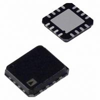
ADA4932-1YCPZ-RL Analog Devices Inc, ADA4932-1YCPZ-RL Datasheet - Page 23

ADA4932-1YCPZ-RL
Manufacturer Part Number
ADA4932-1YCPZ-RL
Description
Lw Cst/Lw Pwr Diff ADC Driver
Manufacturer
Analog Devices Inc
Datasheet
1.ADA4932-1YCPZ-R7.pdf
(28 pages)
Specifications of ADA4932-1YCPZ-RL
Design Resources
Single-Ended-to-Differential High Speed Drive Circuit for 16-Bit, 10 MSPS AD7626 ADC (CN0105)
Amplifier Type
Differential
Number Of Circuits
1
Output Type
Differential
Slew Rate
2800 V/µs
-3db Bandwidth
560MHz
Current - Input Bias
2.5µA
Voltage - Input Offset
500µV
Current - Supply
9.6mA
Current - Output / Channel
80mA
Voltage - Supply, Single/dual (±)
3 V ~ 11 V, ±1.5 V ~ 5.5 V
Operating Temperature
-40°C ~ 105°C
Mounting Type
Surface Mount
Package / Case
16-LFCSP
Lead Free Status / RoHS Status
Lead free / RoHS Compliant
Gain Bandwidth Product
-
Lead Free Status / RoHS Status
Lead free / RoHS Compliant
4.
INPUT COMMON-MODE VOLTAGE RANGE
The ADA4932-x input common-mode range is shifted down
by approximately one VBE, in contrast to other ADC drivers
with centered input ranges such as the ADA4939-x. The
downward-shifted input common-mode range is especially
suited to dc-coupled, single-ended-to-differential, and single-
supply applications.
For ±5 V operation, the input common-mode range at the
summing nodes of the amplifier is specified as −4.8 V to +3.2 V,
and is specified as +0.2 V to +3.2 V with a +5 V supply. To
avoid nonlinearities, the voltage swing at the +IN and −IN
terminals must be confined to these ranges.
2V p-p
Figure 63. Terminated Single-Ended-to-Differential System with G = 2
V
The feedback resistor value is modified as a final gain
adjustment to obtain the desired output voltage.
To make the output voltage V
using the following formula:
The closest standard 1% value to 509 Ω is 511 Ω, which
gives a differential output voltage of 1.00 V p-p.
The final circuit is shown in Figure 63.
R
S
F
Desired
50Ω
R
S
V
1V p-p
53.6Ω
OUT
25.5Ω
V
R
R
TH
TS
T
,
dm
499Ω
V
499Ω
R
R
R
OCM
G
G
G
R
TS
ADA4932-x
511Ω
511Ω
OUT
R
R
F
F
+V
–V
1
= 1 V p-p, calculate R
V
S
S
. 1
p
03
p
V
p
524
R
p
5 .
L
V
1.00V p-p
OUT, dm
509
F
Rev. A | Page 23 of 28
INPUT AND OUTPUT CAPACITIVE AC COUPLING
While the ADA4932-x is best suited to dc-coupled applications,
it is nonetheless possible to use it in ac-coupled circuits. Input
ac coupling capacitors can be inserted between the source and
R
feedback current and causes the ADA4932-x dc input common-
mode voltage to equal the dc output common-mode voltage.
These ac coupling capacitors must be placed in both loops to keep
the feedback factors matched. Output ac coupling capacitors can
be placed in series between each output and its respective load.
SETTING THE OUTPUT COMMON-MODE VOLTAGE
The V
tage divider comprised of two 50 kΩ resistors across the supplies,
with a tap at a voltage approximately equal to the midsupply
point, [(+V
V
applied voltage and its associated source resistance. Relying on
the internal bias results in an output common-mode voltage
that is within about 100 mV of the expected value.
In cases where more accurate control of the output common-
mode level is required, it is recommended that an external
source or resistor divider be used with source resistance less
than 100 Ω. If an external voltage divider consisting of equal
resistor values is used to set V
accuracy than produced internally, higher values can be used
because the external resistors are placed in parallel with the
internal resistors. The output common-mode offset listed in the
Specifications section assumes that the V
low impedance voltage source.
It is also possible to connect the V
level (CML) output of an ADC; however, care must be taken to
ensure that the output has sufficient drive capability. The input
impedance of the V
ADA4932-x devices share one ADC reference output, a buffer
may be necessary to drive the parallel inputs.
G
OCM
. This ac coupling blocks the flow of the dc common-mode
pin sources and sinks current, depending on the externally
OCM
pin of the ADA4932-x is internally biased with a vol-
S
) + (−V
S
OCM
)]/2. Because of this internal divider, the
pin is approximately 10 kΩ. If multiple
ADA4932-1/ADA4932-2
OCM
to midsupply with greater
OCM
input to a common-mode
OCM
input is driven by a


