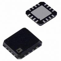
ADA4856-3YCPZ-RL Analog Devices Inc, ADA4856-3YCPZ-RL Datasheet - Page 13

ADA4856-3YCPZ-RL
Manufacturer Part Number
ADA4856-3YCPZ-RL
Description
Triple High Speed Extend Input Range RR
Manufacturer
Analog Devices Inc
Datasheet
1.ADA4856-3YCPZ-R7.pdf
(20 pages)
Specifications of ADA4856-3YCPZ-RL
Applications
Voltage Feedback
Output Type
Rail-to-Rail
Number Of Circuits
3
-3db Bandwidth
370MHz
Slew Rate
800 V/µs
Current - Supply
7.8mA
Current - Output / Channel
52mA
Voltage - Supply, Single/dual (±)
3 V ~ 5.5 V, ±1.5 V ~ 2.75 V
Mounting Type
Surface Mount
Package / Case
16-VQFN, CSP Exposed Pad
Lead Free Status / RoHS Status
Lead free / RoHS Compliant
APPLICATIONS INFORMATION
USING THE ADA4856-3 IN GAINS EQUAL TO +1, −1
The ADA4856-3 was designed to offer outstanding video
performance, simplify applications, and minimize board area.
The ADA4856-3 is a triple amplifier with on-chip feedback
and gain set resistors. The gain is fixed internally at G = +2. The
inclusion of the on-chip resistors not only simplifies the design of
the application but also eliminates six surface-mount resistors,
saving valuable board space and lowering assembly costs.
Whereas the ADA4856-3 has a fixed gain of G = +2, it can be
used in other gain configurations, such as G = −1 and G = +1.
Unity-Gain Operation
Option 1
There are two options for obtaining unity gain (G = +1). The
first is shown in Figure 34. In this configuration, the –IN input
pin is tied to the output (feedback is now provided with the two
internal 402 Ω resistors in parallel), and the input is applied to
the noninverting input. The noise gain for this configuration is 1.
Option 2
Another option exists for running the ADA4856-3 as a unity-
gain amplifier. In this configuration, the noise gain is +2, see
Figure 35. The frequency response and transient response for
this configuration closely match the gain of +2 plots because the
noise gains are equal. This method does have twice the noise gain
of Option 1; however, in applications that do not require low noise,
Option 2 offers less peaking and ringing. By tying the inputs
together, the net gain of the amplifier becomes 1. Equation 1 shows
the transfer characteristic for the schematic shown in Figure 35.
which simplifies to V
V
OUT
=
V
V
IN
IN
⎛ −
⎜
⎜
⎝
Figure 34. Unity Gain of Option 1
R
R
G
R
OUT
F
T
⎞
⎟
⎟
⎠
+
= V
V
IN
IN
.
⎛
⎜
⎜
⎝
GAIN OF +1
R
F
+V
–V
R
+
S
S
G
0.1µF
10µF
0.1µF
10µF
R
G
⎞
⎟
⎟
⎠
V
OUT
Rev. A | Page 13 of 20
(1)
Inverting Unity-Gain Operation
In this configuration, the noninverting input is tied to ground
and the input signal is applied to the inverting input. The noise
gain for this configuration is +2, see Figure 36.
Figure 37 shows the small signal frequency response for both
gain of +1 (Option 1 and Option 2) and gain of −1 configurations.
It is clear that G = +1, Option 2 has better flatness and no peaking
compared to Option 1.
–12
–3
–6
–9
6
3
0
1
V
R
V
S
OUT
L
V
= 5V
= 100Ω
IN
V
IN
Figure 36. Inverting Configuration (G = −1)
= 100mV p-p
Figure 35. Unity Gain of Option 2
R
T
R
Figure 37. G = +1 and G = −1
T
10
FREQUENCY (MHz)
R
G
GAIN OF +1
GAIN OF –1
R
F
+V
–V
S
S
+V
–V
0.1µF
0.1µF
10µF
10µF
S
S
0.1µF
OPTION 2
G = +1
0.1µF
10µF
10µF
100
G = –1
V
OUT
ADA4856-3
V
OPTION 1
G = +1
OUT
1000


