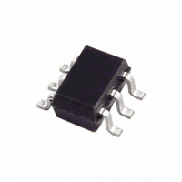
ADA4853-1AKSZ-R2 Analog Devices Inc, ADA4853-1AKSZ-R2 Datasheet - Page 5

ADA4853-1AKSZ-R2
Manufacturer Part Number
ADA4853-1AKSZ-R2
Description
IC,Operational Amplifier,SINGLE,BIPOLAR,TSSOP,6PIN,PLASTIC
Manufacturer
Analog Devices Inc
Datasheet
1.ADA4853-1AKSZ-R2.pdf
(20 pages)
Specifications of ADA4853-1AKSZ-R2
Applications
Voltage Feedback
Output Type
Rail-to-Rail
Number Of Circuits
1
-3db Bandwidth
100MHz
Slew Rate
120 V/µs
Current - Supply
1.4mA
Current - Output / Channel
160mA
Voltage - Supply, Single/dual (±)
2.65 V ~ 5 V
Mounting Type
Surface Mount
Package / Case
6-TSSOP, SC-88, SOT-363
Lead Free Status / RoHS Status
Lead free / RoHS Compliant
Other names
ADA4853-1AKSZ-R2TR
Available stocks
Company
Part Number
Manufacturer
Quantity
Price
Company:
Part Number:
ADA4853-1AKSZ-R2
Manufacturer:
Analog Devices Inc
Quantity:
1 984
SPECIFICATIONS WITH 5 V SUPPLY
T
Table 2.
Parameter
DYNAMIC PERFORMANCE
NOISE/DISTORTION PERFORMANCE
DC PERFORMANCE
INPUT CHARACTERISTICS
DISABLE
OUTPUT CHARACTERISTICS
A
−3 dB Bandwidth
Bandwidth for 0.5 dB Flatness
Settling Time to 0.1%
Slew Rate
Differential Gain
Differential Phase
Input Voltage Noise
Input Current Noise
Crosstalk
Input Offset Voltage
Input Offset Voltage Drift
Input Bias Current
Input Bias Current Drift
Input Bias Offset Current
Open-Loop Gain
Input Resistance
Input Capacitance
Input Common-Mode Voltage Range
Input Overdrive Recovery Time
(Rise/Fall)
Common-Mode Rejection Ratio
DISABLE Input Voltage
Turn-Off Time
Turn-On Time
DISABLE Bias Current
Output Overdrive Recovery Time
Output Voltage Swing
Short-Circuit Current
= 25°C, R
Enabled
Disabled
F
= 1 kΩ, R
G
= 1 kΩ for G = +2, R
Conditions
G = +1, V
G = +2, V
G = +2, V
V
G = +2, V
ADA4853-3W only: T
R
R
f = 100 kHz
f = 100 kHz
G = +2, V
ADA4853-3W only: T
ADA4853-3W only: T
V
ADA4853-3W only: T
Differential/common mode
V
V
ADA4853-3W only: T
DISABLE = 5 V
DISABLE = 5 V, ADA4853-3W only:
T
DISABLE = 0 V
V
R
R
Sinking/sourcing
MIN
O
L
L
O
IN
CM
IN
L
L
= 150 Ω
= 150 Ω
= 75 Ω
= 75 Ω, ADA4853-3W only: T
L
= 2 V step
= 0.5 V to 4.5 V
= −0.5 V to +5.5 V, G = +1
= −0.25 V to +2.75 V, G = +2
= 0 V to 3 V
= 150 Ω, unless otherwise noted.
to T
MAX
O
O
O
O
O
= 2 V p-p, R
= 0.1 V p-p
= 2 V p-p
= 2 V p-p
= 2 V step
Rev. F | Page 5 of 20
MIN
L
MIN
MIN
MIN
MIN
= 150 Ω, f = 5 MHz
to T
to T
to T
to T
to T
MAX
MAX
MAX
MAX
MAX
MIN
to T
MAX
ADA4853-1/ADA4853-2/ADA4853-3
Min
93
70
72
70
−71
−68
0.55 to 4.5
0.55 to 4.5
Typ
100
35
22
54
120
0.22
0.10
22
2.2
−66
1
1.6
1.0
4
60
80
0.5/20
0.6
−0.2 to +V
40
−88
1.2
1.5
120
40
0.01
55
0.1 to 4.8
160/120
CC
− 1.2
Max
4.1
6.0
1.7
1.7
50
50
Unit
MHz
MHz
MHz
ns
V/µs
V/µs
%
Degrees
nV/√Hz
pA/√Hz
dB
mV
mV
µV/°C
µA
µA
nA/°C
nA
dB
dB
MΩ
pF
V
ns
dB
dB
V
µs
ns
µA
µA
µA
ns
V
V
mA


