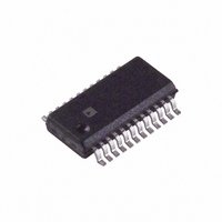
ADA4411-3ARQZ-R7 Analog Devices Inc, ADA4411-3ARQZ-R7 Datasheet

ADA4411-3ARQZ-R7
Specifications of ADA4411-3ARQZ-R7
Related parts for ADA4411-3ARQZ-R7
ADA4411-3ARQZ-R7 Summary of contents
Page 1
... LEVEL2 CUTOFF SELECT GAIN SELECT DISABLE The ADA4411-3 can operate on a single +5 V supply as well as on ±5 V supplies. Single-supply operation is ideal in applications where power consumption is critical. The disable feature allows for further power conservation by reducing the supply current to typically 15 μA when a particular device is not in use ...
Page 2
... ADA4411-3 TABLE OF CONTENTS Features .............................................................................................. 1 Applications....................................................................................... 1 Functional Block Diagram .............................................................. 1 General Description ......................................................................... 1 Revision History ............................................................................... 2 Specifications..................................................................................... 3 Absolute Maximum Ratings............................................................ 5 Thermal Resistance ...................................................................... 5 ESD Caution.................................................................................. 5 Pin Configuration And Function Descriptions............................ 6 Typical Performance Characteristics ............................................. 7 Theory of Operation ...................................................................... 10 Applications..................................................................................... 11 REVISION HISTORY 7/05—Revision 0: Initial Version Overview ..................................................................................... 11 Multiplexer Select Inputs........................................................... 11 Throughput Gain ...
Page 3
... Cutoff frequency select = 18 MHz Cutoff frequency select = 9 MHz NTSC MHz C NTSC MHz C All inputs except DISABLE All inputs except DISABLE All inputs except DISABLE MHz All channels All channels Rev Page ADA4411-3 Min Typ Max Unit ±500 mV V − 0.1 V − 2.0 V S− ...
Page 4
... ADA4411 ± 25° 1 × Table 2. Parameter OVERALL PERFORMANCE Offset Error Offset Adjust Range Input Voltage Range, All Inputs Output Voltage Swing, All Outputs Linear Output Current per Channel Integrated Voltage Noise, Referred to Input Filter Input Bias Current Total Harmonic Distortion at 1 MHz ...
Page 5
... Package Type θ Lead QSOP 83 Maximum Power Dissipation The maximum safe power dissipation in the ADA4411-3 package is limited by the associated rise in junction temperature ( the die. At approximately 150°C, which is the glass J transition temperature, the plastic changes its properties. Even temporarily exceeding this temperature limit may change the stresses that the package exerts on the die, permanently shifting the parametric performance of the ADA4411-3 ...
Page 6
... G_SEL Gain Select 24 LEVEL2 DC Level Adjust Pin 2 LEVEL1 LEVEL2 1 24 DISABLE 2 G_SEL 23 Y1/ VCC GND 4 21 Y/G_OUT Pb1/B1 VEE 5 20 ADA4411-3 GND Pb/B_OUT 6 19 TOP VIEW (Not to Scale) Pr1/ VEE F_SEL_A Pr/R_OUT 8 17 F_SEL_B VCC 9 16 Y2/G2 MUX 10 15 DGND 11 14 ...
Page 7
... FREQUENCY (MHz) Figure 7. Frequency Response vs. Power Supply and Cutoff Frequency (G = × 9MHz 18MHz C BLACK LINE +5V S GRAY LINE ±5V S 9.5 9 FREQUENCY (MHz × 36MHz 9MHz –3 C –6 – 18MHz C –40°C +25°C +85° 100 FREQUENCY (MHz) ADA4411 36MHz C 100 ...
Page 8
... ADA4411-3 100 9MHz 18MHz 36MHz FREQUENCY (MHz) Figure 10. Group Delay vs. Frequency, Power Supply, and Cutoff Frequency – 300Ω SOURCE Y AND Pr SOURCE CHANNELS –40 Pb RECEPTOR CHANNEL –50 – 9MHz C –70 –80 –90 –100 –110 0 FREQUENCY (MHz) Figure 11. Channel-to-Channel Crosstalk vs. Frequency and Cutoff Frequency 3 ...
Page 9
... Figure 18. Negative Supply PSRR vs. Frequency and Cutoff Frequency NETWORK ANALYZER Tx 50Ω MINIMUM-LOSS MATCHING NETWORK LOSS CALIBRATED OUT 200ns/DIV Figure 19. Basic Test Circuit for Swept Frequency Measurements Rev Page ADA4411 18MHz 9MHz 36MHz 100 FREQUENCY (MHz) ...
Page 10
... In applications where power consumption is critical, the part can be powered down to draw typically 15 μA by pulling the DISABLE pin to the most positive rail. The ADA4411-3 is also well-suited for high encoding frequency applications because it maintains a stop-band attenuation of more than 400 MHz. ...
Page 11
... G_SEL pin. Table 6 summarizes how the gain is selected. DISABLE The ADA4411-3 includes a disable feature that can be used to save power when a particular device is not in use. As indicated in the Overview section, the disable feature is asserted by pulling the DISABLE pin to the positive supply. ...
Page 12
... Figure 21. Flexible Circuits to Set the LEVEL1 and LEVEL2 Inputs to Obtain a 600 mV Output Offset on a Single Supply INPUT AND OUTPUT COUPLING Inputs to the ADA4411-3 are normally dc-coupled. Ac coupling the inputs is not recommended; however coupling is necessary, suitable circuitry must be provided following the ac coupling element to provide proper dc level and bias currents at the ADA4411-3 input stages ...
Page 13
... VIDEO ENCODER RECONSTRUCTION FILTER The ADA4411-3 is easily applied as a reconstruction filter at the DAC outputs of a video encoder. Figure 24 illustrates how to use the ADA4411-3 in this type of application with an ADV7322 video encoder in a single-supply application with ac-coupled outputs. Rev Page ...
Page 14
... ADA4411-3 ADV7322 VIDEO ENCODER VIDEO DAC OUTPUTS CHANNEL 2 VIDEO INPUTS Figure 24. The ADA4411-3 Applied as a Single-Supply Reconstruction Filter Following the ADV7322 0.1μF DNP 10kΩ 0.1μF 0Ω 634Ω 1 LEVEL1 24 LEVEL2 0.1μF 2 DISABLE 23 G_SEL 15 BINARY MUX CONTROL 8 INPUTS ...
Page 15
... OUTLINE DIMENSIONS PIN 1 0.010 0.004 COPLANARITY ORDERING GUIDE Model Temperature Range ADA4411-3ARQZ 1 –40°C to +85°C 1 ADA4411-3ARQZ-R7 –40°C to +85°C 1 ADA4411-3ARQZ-RL –40°C to +85° Pb-free part. 0.341 BSC 24 13 0.154 BSC 1 12 0.065 0.069 0.049 0.053 0.025 0.012 SEATING BSC 0 ...
Page 16
... ADA4411-3 NOTES © 2005 Analog Devices, Inc. All rights reserved. Trademarks and registered trademarks are the property of their respective owners. D05527–0–7/05(0) Rev Page ...


