AD9957BSVZ-REEL Analog Devices Inc, AD9957BSVZ-REEL Datasheet - Page 3
AD9957BSVZ-REEL
Manufacturer Part Number
AD9957BSVZ-REEL
Description
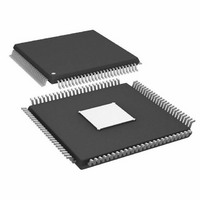
IC,RF Modulator,TQFP,100PIN,PLASTIC
Manufacturer
Analog Devices Inc
Datasheet
1.AD9957BSVZ-REEL.pdf
(64 pages)
Specifications of AD9957BSVZ-REEL
Resolution (bits)
14 b
Master Fclk
1GHz
Tuning Word Width (bits)
32 b
Voltage - Supply
1.8V, 3.3V
Operating Temperature
-40°C ~ 85°C
Mounting Type
Surface Mount
Package / Case
100-TQFP Exposed Pad, 100-eTQFP, 100-HTQFP, 100-VQFP
Operating Temperature (max)
85C
Operating Temperature (min)
-40C
Pin Count
100
Mounting
Surface Mount
Case Height
1mm
Screening Level
Industrial
Lead Free Status / RoHS Status
Lead free / RoHS Compliant
For Use With
AD9957/PCBZ - BOARD EVAL AD9957 QUADRATURE MOD
Lead Free Status / Rohs Status
Compliant
Available stocks
Company
Part Number
Manufacturer
Quantity
Price
Company:

Part Number:
AD9957BSVZ-REEL
Manufacturer:
Analog Devices Inc
Quantity:
10 000
Part Number:
AD9957BSVZ-REEL
Manufacturer:
ADI/亚德诺
Quantity:
20 000


Power Supply Partitioning ............................................................. 46
Serial Programming ........................................................................ 47
Sync Generator ............................................................................ 40
Sync Receiver ............................................................................... 41
Setup/Hold Validation ................................................................ 42
Synchronization Example .......................................................... 44
I/Q Path Latency ......................................................................... 45
3.3 V Supplies .............................................................................. 46
1.8 V Supplies .............................................................................. 46
Control Interface—Serial I/O .................................................... 47
General Serial I/O Operation .................................................... 47
Instruction Byte ........................................................................... 47
Serial I/O Port Pin Descriptions ............................................... 47
Example .................................................................................... 45
DVDD_I/O (Pin 11, Pin 15, Pin 21, Pin 28, Pin 45, Pin 56,
Pin 66) ...................................................................................... 46
AVDD (Pin 74 to Pin 77 and Pin 83) .................................. 46
DVDD (Pin 17, Pin 23, Pin 30, Pin 47, Pin 57, Pin 64) ..... 46
AVDD (Pin 3) .......................................................................... 46
AVDD (Pin 6) .......................................................................... 46
AVDD (Pin 89 and Pin 92) .................................................... 46
Instruction Byte Information Bit Map ................................. 47
SCLK—Serial Clock................................................................ 47
CS —Chip Select Bar ............................................................... 47
SDIO—Serial Data Input/Output ......................................... 47
SDO—Serial Data Out ........................................................... 48
Rev. B | Page 3 of 64
Register Map and Bit Descriptions ............................................... 50
Outline Dimensions ........................................................................ 61
Serial I/O Timing Diagrams ...................................................... 48
MSB/LSB Transfers ..................................................................... 48
I/O_UPDATE, SYNC_CLK, and System Clock
Relationships................................................................................ 49
Register Map ................................................................................ 50
Register Bit Descriptions............................................................ 55
Profile Registers ........................................................................... 60
Ordering Guide ........................................................................... 61
I/O_RESET—Input/Output Reset ........................................ 48
I/O_UPDATE—Input/Output Update ................................ 48
Control Function Register 1 (CFR1) .................................... 55
Control Function Register 2 (CFR2) .................................... 56
Control Function Register 3 (CFR3) .................................... 58
Auxiliary DAC Control Register ........................................... 58
I/O Update Rate Register ....................................................... 58
RAM Segment Register 0 ....................................................... 58
RAM Segment Register 1 ....................................................... 59
Amplitude Scale Factor (ASF) Register ............................... 59
Multichip Sync Register ......................................................... 59
Profile<7:0> Register—Single Tone ...................................... 60
Profile<7:0> Register—QDUC ............................................. 60
RAM Register .......................................................................... 60
GPIO Configuration Register ............................................... 60
GPIO Data Register ................................................................ 60
AD9957
Related parts for AD9957BSVZ-REEL
Image
Part Number
Description
Manufacturer
Datasheet
Request
R

Part Number:
Description:
D/A Converter Evaluation Board
Manufacturer:
Analog Devices Inc
Datasheet:

Part Number:
Description:
1 GSPS Quadrature Digital Upconverter
Manufacturer:
Analog Devices
Datasheet:

Part Number:
Description:
±1.7g Dual-Axis IMEMS Accelerometer Evaluation Board
Manufacturer:
Analog Devices Inc
Datasheet:

Part Number:
Description:
Inertial Sensor Evaluation System
Manufacturer:
Analog Devices Inc
Datasheet:
Part Number:
Description:
Manufacturer:
Analog Devices Inc
Datasheet:
Part Number:
Description:
Manufacturer:
Analog Devices Inc
Datasheet:
Part Number:
Description:
Manufacturer:
Analog Devices Inc
Datasheet:
Part Number:
Description:
Manufacturer:
Analog Devices Inc
Datasheet:
Part Number:
Description:
Manufacturer:
Analog Devices Inc
Datasheet:
Part Number:
Description:
Manufacturer:
Analog Devices Inc
Datasheet:
Part Number:
Description:
Manufacturer:
Analog Devices Inc
Datasheet:
Part Number:
Description:
Manufacturer:
Analog Devices Inc
Datasheet:
Part Number:
Description:
Manufacturer:
Analog Devices Inc
Datasheet: