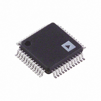
AD9952YSVZ-REEL7 Analog Devices Inc, AD9952YSVZ-REEL7 Datasheet - Page 7

AD9952YSVZ-REEL7
Manufacturer Part Number
AD9952YSVZ-REEL7
Description
IC,FREQUENCY SYNTHESIZER,CMOS,TQFP,48PIN,PLASTIC
Manufacturer
Analog Devices Inc
Datasheet
1.AD9952YSVZ.pdf
(28 pages)
Specifications of AD9952YSVZ-REEL7
Resolution (bits)
14 b
Master Fclk
400MHz
Tuning Word Width (bits)
32 b
Voltage - Supply
1.71 V ~ 1.96 V
Operating Temperature
-40°C ~ 105°C
Mounting Type
Surface Mount
Package / Case
48-TQFP Exposed Pad, 48-eTQFP, 48-HTQFP, 48-VQFP
Lead Free Status / RoHS Status
Lead free / RoHS Compliant
For Use With
AD9952/PCB - BOARD EVAL FOR AD9952
Lead Free Status / Rohs Status
Compliant
Available stocks
Company
Part Number
Manufacturer
Quantity
Price
Company:
Part Number:
AD9952YSVZ-REEL7
Manufacturer:
Analog Devices Inc
Quantity:
10 000
PIN CONFIGURATION AND FUNCTION DESCRIPTIONS
Note that the exposed paddle on the bottom of the package is a ground connection for the DAC and must be attached to AGND in
any board layout. Note that Pin 43, DVDD_I/O, can be powered to 1.8 V or 3.3 V; however, the DVDD pins (Pin 2 and Pin 34) can
only be powered to 1.8 V.
Table 3. 48-Lead TQFP/EP
Pin No.
1
2, 34
3, 33, 42,
47, 48
4, 6, 13,
16, 18, 19,
25, 27, 29
5, 7, 14,
15, 17, 22,
26, 32
8
9
10
11
12
20
21
Mnemonic
I/O UPDATE
DVDD
DGND
AVDD
AGND
REFCLK
REFCLK
CRYSTAL OUT
CLKMODESELECT
LOOP_FILTER
IOUT
IOUT
CLKMODESELECT
CRYSTAL OUT
LOOP_FILTER
I/O UPDATE
I/O
I
I
I
I
I
I
I
O
I
I
O
O
REFCLK
REFCLK
DGND
AGND
AGND
DVDD
AVDD
AVDD
Description
The rising edge transfers the contents of the internal buffer memory to the I/O registers. This pin
must be set up and held around the SYNC_CLK output signal.
Digital Power Supply Pins (1.8 V).
Digital Power Ground Pins.
Analog Power Supply Pins (1.8 V).
Analog Power Ground Pins.
Complementary Reference Clock/Oscillator Input. When the REFCLK port is operated in single-
ended mode, REFCLK should be decoupled to AVDD with a 0.1 µF capacitor.
Reference Clock/Oscillator Input. See the Clock Input section for details on the oscillator/REFCLK
operation.
Output of the Oscillator Section.
Control Pin for the Oscillator Section. When high, the oscillator section is enabled. When low, the
oscillator section is bypassed.
This pin provides the connection for the external zero compensation network of the REFCLK
multiplier’s PLL loop filter. The network consists of a 1 k Ω resistor in series with a 0.1 µF capacitor
tied to AVDD.
Complementary DAC Output. Should be biased through a resistor to AVDD, not AGND.
DAC Output. Should be biased through a resistor to AVDD, not AGND.
10
11
12
1
2
3
4
5
6
7
8
9
48
13
47
14
15
46
Figure 2. Pin Configuration
16
45
Rev. B | Page 7 of 28
17
44
(Not to Scale)
AD9952
TOP VIEW
43
18
19
42
41
20
40 39
21 22
38
23
37
24
36
35
34
33
32
30
29
28
27
26
25
31
RESET
PWRDWNCTL
DVDD
DGND
AGND
COMP_IN
COMP_IN
AVDD
COMP_OUT
AVDD
AGND
AVDD
AD9952


