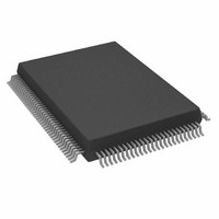
AD9888KSZ-100 Analog Devices Inc, AD9888KSZ-100 Datasheet - Page 5

AD9888KSZ-100
Manufacturer Part Number
AD9888KSZ-100
Description
IC,TV/VIDEO CIRCUIT,Video Digitizer,CMOS,QFP,128PIN,PLASTIC
Manufacturer
Analog Devices Inc
Datasheet
1.AD9888KSZ-205.pdf
(32 pages)
Specifications of AD9888KSZ-100
Applications
Graphic Cards, VGA Interfaces
Interface
2-Wire Serial
Voltage - Supply
3 V ~ 3.6 V
Package / Case
128-MQFP, 128-PQFP
Mounting Type
Surface Mount
Lead Free Status / RoHS Status
Lead free / RoHS Compliant
Available stocks
Company
Part Number
Manufacturer
Quantity
Price
Company:
Part Number:
AD9888KSZ-100
Manufacturer:
AD
Quantity:
494
Company:
Part Number:
AD9888KSZ-100
Manufacturer:
Analog Devices Inc
Quantity:
10 000
Part Number:
AD9888KSZ-100
Manufacturer:
ADI/亚德诺
Quantity:
20 000
Part Number:
AD9888KSZ-100 (AD80094)
Manufacturer:
ADI/亚德诺
Quantity:
20 000
Pin Type
Analog Video Inputs R
Sync/Clock Inputs
Sync Outputs
Voltage
Clamp Voltages
PLL Filter
Power Supply
Serial Port
(2-Wire
Serial Interface)
Data Outputs
Data Clock
Output
REV. B
Mnemonic
G
B
R
G
B
HSYNC0
VSYNC0
SOGIN0
HSYNC1
VSYNC1
SOGIN1
CLAMP
COAST
CKEXT
CKINV
HSOUT
VSOUT
SOGOUT
REF BYPASS
RMIDSCV
BMIDSCV
FILT
V
V
PV
GND
SDA
SCL
A0
Red A[7:0]
Red B[7:0]
Green A[7:0]
Green B[7:0]
Blue A[7:0]
Blue B[7:0]
DATACK
DATACK
AIN
AIN
AIN
AIN
D
DD
AIN
AIN
D
0
0
1
1
0
1
Function
Channel 0 Analog Input for Converter R
Channel 0 Analog Input for Converter G
Channel 0 Analog Input for Converter B
Channel 1 Analog Input for Converter R
Channel 1 Analog Input for Converter G
Channel 1 Analog Input for Converter B
Channel 0 Horizontal SYNC Input
Channel 0 Vertical SYNC Input
Channel 0 Input for Sync-on-Green
Channel 1 Horizontal SYNC Input
Channel 1 Vertical SYNC Input
Channel 1 Input for Sync-on-Green
Clamp Input (External CLAMP signal)
PLL Coast Signal Input
External Pixel Clock Input (to Bypass the PLL) or 10 kΩ to Ground
ADC Sampling Clock Invert
HSYNC Output Clock (Phase-Aligned with DATACK)
VSYNC Output Clock (Phase-Aligned with DATACK)
Sync-on-Green Slicer Output
Internal Reference Bypass (Bypass with 0.1 µF to Ground)
Red Channel Midscale Clamp Voltage Bypass
Blue Channel Midscale Clamp Voltage Bypass
Connection for External Filter Components for Internal PLL
Analog Power Supply
Output Power Supply
PLL Power Supply
Ground
Serial Port Data I/O
Serial Port Data Clock
Serial Port Address Input 1
Port A Outputs of Converter “Red.” Bit 7 is the MSB.
Port B Outputs of Converter “Red.” Bit 7 is the MSB.
Port A Outputs of Converter “Green.” Bit 7 is the MSB.
Port B Outputs of Converter “Green.” Bit 7 is the MSB.
Port A Outputs of Converter “Blue.” Bit 7 is the MSB.
Port B Outputs of Converter “Blue.” Bit 7 is the MSB.
Data Output Clock
Data Output Clock Complement
Table I. Complete Pinout List
–5–
Value
0.0 V to 1.0 V 5
0.0 V to 1.0 V 13
0.0 V to 1.0 V 20
0.0 V to 1.0 V 8
0.0 V to 1.0 V 17
0.0 V to 1.0 V 23
3.3 V CMOS
3.3 V CMOS
0.0 V to 1.0 V 12
3.3 V CMOS
3.3 V CMOS
0.0 V to 1.0 V 16
3.3 V CMOS
3.3 V CMOS
3.3 V CMOS
3.3 V CMOS
3.3 V CMOS
3.3 V CMOS
3.3 V CMOS
1.25 V ± 10% 2
3.3 V ± 10%
3.3 V ± 10%
3.3 V ± 10%
0 V
3.3 V CMOS
3.3 V CMOS
3.3 V CMOS
3.3 V CMOS
3.3 V CMOS
3.3 V CMOS
3.3 V CMOS
3.3 V CMOS
3.3 V CMOS
3.3 V CMOS
3.3 V CMOS
AD9888
Pin No.
45
44
43
42
30
53
54
29
125
127
126
9
24
50
31
32
33
113–120
103–110
90–97
80–87
70–77
57–64
123
124


