AD9850/FSPCB Analog Devices Inc, AD9850/FSPCB Datasheet
AD9850/FSPCB
Specifications of AD9850/FSPCB


Related parts for AD9850/FSPCB


AD9850/FSPCB Summary of contents
Page 1
FEATURES 125 MHz Clock Rate On-Chip High Performance DAC and High Speed Comparator DAC SFDR > MHz A 32-Bit Frequency Tuning Word Simplified Control Interface: Parallel Byte or Serial Loading Format Phase Modulation Capability 3.3 ...
Page 2
AD9850–SPECIFICATIONS Parameter CLOCK INPUT CHARACTERISTICS Frequency Range 5 V Supply 3.3 V Supply Pulse Width High/Low 5 V Supply 3.3 V Supply DAC OUTPUT CHARACTERISTICS Full-Scale Output Current R = 3.9 kΩ SET R = 1.95 kΩ SET Gain Error ...
Page 3
Parameter CMOS LOGIC INPUTS (Including CLKIN) Logic 1 Voltage Supply Logic 1 Voltage, 3.3 V Supply Logic 0 Voltage Logic 1 Current Logic 0 Current Input Capacitance POWER SUPPLY (A = 1/3 CLKIN) OUT +V Current @ S ...
Page 4
... AD9850BRS –40°C to +85°C AD9850BRS-REEL –40°C to +85°C AD9850BRSZ* –40°C to +85°C AD9850BRSZ-REEL* –40°C to +85°C AD9850/CGPCB AD9850/FSPCB *Z = Pb-free part. EXPLANATION OF TEST LEVELS Test Level I 100% Production Tested. III Sample Tested Only Parameter is guaranteed by design and characterization testing ...
Page 5
Pin No. Mnemonic Function 8-Bit Data Input. This is the 8-bit data port for iteratively loading the 32-bit frequency and the 8-bit phase control word MSB LSB. ...
Page 6
AD9850–Typical Performance Characteristics Spectrum CH1 S 10dB/REF –8.6dBm CLOCK 125MHz AD9850 0 RBW # 100Hz VBW 100Hz ATN # 30dB SWP START 0Hz TPC 1. SFDR, CLKIN = 125 MHz/f CH1 S Spectrum –10dBm 10dB/REF CLOCK 125MHz AD9850 0 RBW ...
Page 7
Tek Run: 50.0GS/s ET Average 1 Ch1 1.00V TPC 7. Comparator Output Rise Time (5 V Supply/15 pF Load 3. CLKIN – MHz ...
Page 8
AD9850 +V GND S IOUT 8-b 5 PARALLEL DATA, OR 1-b 40 SERIAL DATA, DATA PROCESSOR RESET, AND 2 BUS CLOCK LINES AD9850 IOUTB VINN XTAL CLK VINP OSC QOUT QOUTB RSET Figure 1. Basic AD9850 Clock Generator Application with ...
Page 9
N ACCUMULATOR TUNING WORD SPECIFIES OUTPUT FREQUENCY AS A FRACTION OF REF CLOCK FREQUENCY Figure 4. Basic DDS Block Diagram and Signal Flow of AD9850 AD9850 is a sampled signal, its output spectrum follows the Nyquist sampling theorem. Specifically, its ...
Page 10
AD9850 Table II. Factory Reserved Internal Test Control Codes W0* DATA CLK FQ UD CLKIN COS OUT *OUTPUT UPDATE CAN OCCUR AFTER ANY WORD LOAD AND IS ASYNCHRONOUS WITH THE REFERENCE CLOCK Figure 6. Parallel ...
Page 11
CLKIN RESET COS OUT NOTE: THE TIMING DIAGRAM ABOVE SHOWS THE MINIMAL AMOUNT OF RESET TIME NEEDED BEFORE WRITING TO THE DEVICE. HOWEVER, THE MASTER RESET DOES NOT HAVE TO BE SYNCHRONOUS WITH THE CLKIN IF THE MINIMAL TIME IS ...
Page 12
AD9850 DATA (W0) (PARALLEL) REQUIRED TO RESET CONTROL REGISTERS W CLK FQ UD NOTE: FOR DEVICE START-UP IN SERIAL MODE, HARDWIRE PIN PIN AND PIN (SEE FIGURE 11). Figure 11. Pins ...
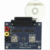
Page 13
... Two versions of evaluation boards are available for the AD9850, which facilitate the implementation of the device for bench- top analysis and serve as a reference for PCB layout. The AD9850/FSPCB is used in applications where the device is used primarily as a frequency synthesizer. This version facilitates connection of the AD9850’s internal D/A converter output Ω ...
Page 14
... Other operational modes (frequency sweeping, sleep, serial input) are available to the user via keyboard/mouse control. The AD9850/FSPCB provides access into and out of the on-chip comparator via test point pairs (each pair has an active input and a ground connection). The two active inputs are labeled TP1 and TP2 ...
Page 15
... 0.1 F 0.1 F 0 Figure 15. AD9850/FSPCB Electrical Schematic AD9850BRS (28-Lead SSOP) 74HCT574 H-CMOS Octal Flip-Flop 0.1 µF Ceramic Chip Capacitor 10 µF Tantalum Chip Capacitor 3.9 kΩ Resistor 50 Ω Resistor 2.2 kΩ Resistor 25 Ω Resistor 1 kΩ Resistor 36-Pin D Connector Banana Jack BNC Connector – ...
Page 16
... AD9850 16a. AD9850/FSPCB Top Layer 16b. AD9850/FSPCB Ground Plane Figure 16. AD9850/FSPCB Evaluation Board Layout 16c. AD9850/FSPCB Power Plane 16d. AD9850/FSPCB Bottom Layer –16– REV. H ...
Page 17
C36CRPX J1 U2 74HCT574 1 RRESET ...
Page 18
AD9850 18a. AD9850/CGPCB Top Layer 18b. AD9850/CGPCB Ground Plane Figure 18. AD9850/CGPCB Evaluation Board Layout 18c. AD9850/CGPCB Power Plane 18d. AD9850/CGPCB Bottom Layer –18– REV. H ...
Page 19
MAX 0.05 MIN REV. H OUTLINE DIMENSIONS 28-Lead Shrink Small Outline Package [SSOP] (RS-28) Dimensions shown in millimeters 10.50 10.20 9. 5.60 8.20 5.30 7.80 5.00 7. 1.85 1.75 0.10 COPLANARITY 1.65 0.25 0.09 0.65 ...
Page 20
AD9850 Revision History Location 2/04—Data Sheet changed from REV REV. H. Changes to SPECIFICATIONS . . . . . . . . . . . . . . . . . . . . . . . . ...