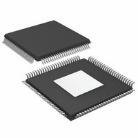
AD9778ABSVZRL Analog Devices Inc, AD9778ABSVZRL Datasheet - Page 28

AD9778ABSVZRL
Manufacturer Part Number
AD9778ABSVZRL
Description
IC,D/A CONVERTER,DUAL,14-BIT,CMOS,TQFP,100PIN
Manufacturer
Analog Devices Inc
Datasheet
1.AD9776ABSVZ.pdf
(60 pages)
Specifications of AD9778ABSVZRL
Number Of Bits
14
Data Interface
Parallel
Number Of Converters
2
Voltage Supply Source
Analog and Digital
Power Dissipation (max)
300mW
Operating Temperature
-40°C ~ 85°C
Mounting Type
Surface Mount
Package / Case
100-TQFP Exposed Pad, 100-eTQFP, 100-HTQFP, 100-VQFP
Lead Free Status / RoHS Status
Lead free / RoHS Compliant
For Use With
AD9778A-EBZ - BOARD EVALUATION AD9778A
Settling Time
-
Lead Free Status / RoHS Status
Lead free / RoHS Compliant
Available stocks
Company
Part Number
Manufacturer
Quantity
Price
Company:
Part Number:
AD9778ABSVZRL
Manufacturer:
Analog Devices Inc
Quantity:
10 000
AD9776A/AD9778A/AD9779A
Register Name
Sync Control
Register
Address
0x03
0x03
0x03
0x03
0x04
0x04
0x04
0x05
0x05
0x05
0x06
0x06
0x07
0x07
0x07
0x07
Bits
7
6
5:4
3:0
7:4
3:1
0
7:4
3:1
0
7:4
3:0
7
6
5
4:0
Parameter
DATACLK Delay Mode
Reserved
DATACLK Divide<1:0>
Data Timing Margin<3:0>
DATACLK Delay<3:0>
SYNC_O Divide<2:0>
SYNC_O Delay<4>
SYNC_O Delay<3:0>
SYNC_I Ratio<2:0>
SYNC_I Delay<4>
SYNC_I Delay<3:0>
SYNC_I Timing Margin<3:0>
SYNC_I Enable
SYNC_O Enable
SYNC_O Triggering Edge
Clock State<4:0>
Rev. A | Page 28 of 60
Function
1: automatic data timing error correct mode
Should always be set to 1.
DATACLK output divider value.
00: divide by 1
01: divide by 2
10: divide by 4
11: divide by 1
Sets the timing margin required to prevent the
Data Timing Error IRQ from being asserted. See
Table 26 for details.
Sets delay of REFCLK in to DATACLK out.
The frequency of the SYNC_O signal is equal to
f
000: N = 32
001: N = 16
010: N = 8
011: N = 4
100: N = 2
101: N = 1
110: N = undefined
111: N = undefined
This value programs the value of the delay line of
the SYNC_O signal. The delay of SYNC_O is relative
to REFCLK. The delay line resolution is 80 ps per
step.
0000: nominal delay
0001: adds 80 ps delay to SYNC_O
0010: adds 160 ps delay to SYNC_O
…
1111: Adds 2480 ps delay to SYNC_O
This value controls the number of SYNC_I input
pulses required to generate a synchronization
pulse. See Table 27 for details.
This value programs the value of the delay line
of the SYNC_I signal. The delay line resolution is
190 ps per step.
0000: no added delay
0001: adds 190 ps delay to SYNC_I
0010: adds 380 ps delay to SYNC_I
…
1111: adds 2480 ps delay to SYNC_I
1: enables the SYNC_I input
1: SYNC_O changes on REFCLK rising edge
This value determines the state of the internal
clock generation state machine upon
synchronization.
0: manual data timing error correct mode
1: enables the SYNC_O output
0: SYNC_O changes on REFCLK falling edge
DAC
/N, where N is set as follows:
Default
0
0
00
0000
0000
000
00000
000
00000
0
0
0
0
0


