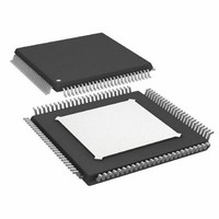
AD9273BSVZ-50 Analog Devices Inc, AD9273BSVZ-50 Datasheet - Page 28

AD9273BSVZ-50
Manufacturer Part Number
AD9273BSVZ-50
Description
12Bit 50 MSPS Octal ADC
Manufacturer
Analog Devices Inc
Type
Crosspoint Switchr
Datasheet
1.AD9273BSVZ-25.pdf
(48 pages)
Specifications of AD9273BSVZ-50
Resolution (bits)
12 b
Sampling Rate (per Second)
50M
Data Interface
Serial
Voltage Supply Source
Single Supply
Voltage - Supply
1.7 V ~ 3.6 V
Operating Temperature
-40°C ~ 85°C
Mounting Type
Surface Mount
Package / Case
100-TQFP Exposed Pad, 100-eTQFP, 100-HTQFP, 100-VQFP
Lead Free Status / RoHS Status
Lead free / RoHS Compliant
Available stocks
Company
Part Number
Manufacturer
Quantity
Price
Company:
Part Number:
AD9273BSVZ-50
Manufacturer:
Analog Devices Inc
Quantity:
10 000
AD9273
Table 9. Sensitivity and Dynamic Range of Trade-Offs
(V/V)
6
8
12
1
2
3
4
5
6
Table 9 demonstrates the sensitivity and dynamic range of
trade-offs that can be achieved relative to various LNA and
VGA gain settings.
For example, when the VGA is set for the minimum gain voltage,
the TGC path is dominated by VGA noise and achieves the
maximum output SNR. However, as the postamp gain options
are increased, the input-referred noise is reduced and the SNR
is degraded.
If the VGA is set for the maximum gain voltage, the TGC path
is dominated by LNA noise and achieves the lowest input-
referred noise, but with degraded output SNR. The higher the
TGC (LNA + VGC) gain, the lower the output SNR. As the
postamp gain is increased, the input-referred noise is reduced.
At low gains, the VGA should limit the system noise perfor-
mance (SNR); at high gains, the noise is defined by the source and
the LNA. The maximum voltage swing is bound by the full-
scale peak-to-peak ADC input voltage (2 V p-p).
Both the LNA and VGA have full-scale limitations within each
section of the TGC path. These limitations are dependent on the
gain setting of each function block and on the voltage applied to the
LNA: output full scale = 4.4 V p-p differential.
Filter: loss ~ 1 dB, NBW = 13.3 MHz, GAIN− = 0.8 V.
ADC: 40 MSPS, 70 dB SNR, 2 V p-p full-scale input.
Output dynamic range at minimum VGA gain (VGA dominated).
Output dynamic range at maximum VGA gain (LNA dominated).
Channel noise at maximum VGA gain.
Gain
(dB)
15.6
17.9
21.3
Full-Scale Input
(V p-p)
0.733
0.550
0.367
LNA
Input-Referred
Noise Voltage
(nV/√Hz)
1.6
1.42
1.26
VGA
Postamp Gain (dB)
21
24
27
30
21
24
27
30
21
24
27
30
1, 2, 3
Rev. B | Page 28 of 48
GAIN+ and GAIN− pins. The LNA has three limitations, or full-
scale settings, that can be applied through the SPI. Similarly, the
VGA has four postamp gain settings that can be applied through
the SPI. The voltage applied to the GAIN± pins determines
which amplifier (the LNA or VGA) saturates first. The maximum
signal input level that can be applied as a function of voltage on
the GAIN± pins for the selectable gain options of the SPI is shown
in Figure 48 to Figure 50.
GAIN+ = 0 V
65.9
64.1
61.8
59.2
65.9
64.1
61.8
59.2
65.9
64.1
61.8
59.2
Typical Output Dynamic Range
Figure 48. LNA with 15.6 dB Gain Setting/VGA Full-Scale Limitations
0.40
0.35
0.30
0.25
0.20
0.15
0.10
0.05
0
0
PGA GAIN = 27dB
4
0.2
PGA GAIN = 30dB
GAIN+ = 1.6 V
62.3
59.7
57.0
54.1
61.6
58.9
56.2
53.3
60.1
57.3
54.4
51.5
0.4
0.6
Channel
GAIN+ (V)
0.8
5
PGA GAIN = 21dB
Input-Referred Noise
GAIN+ = 1.6 V (nV/√Hz)
1.98
1.91
1.87
1.85
1.66
1.61
1.58
1.57
1.35
1.32
1.31
1.30
1.0
PGA GAIN = 24dB
1.2
1.4
1.6
6
@


