AD9272BSVZ-80 Analog Devices Inc, AD9272BSVZ-80 Datasheet - Page 32
AD9272BSVZ-80
Manufacturer Part Number
AD9272BSVZ-80
Description
12Bit 80 MSPS Octal ADC
Manufacturer
Analog Devices Inc
Type
Ultrasound Receiversr
Datasheet
1.AD9272BSVZ-80.pdf
(44 pages)
Specifications of AD9272BSVZ-80
Design Resources
Powering AD9272 with ADP5020 Switching Regulator PMU for Increased Efficiency (CN0135)
Resolution (bits)
12 b
Sampling Rate (per Second)
80M
Data Interface
Serial
Voltage Supply Source
Analog and Digital
Voltage - Supply
1.8V, 3V
Operating Temperature
-40°C ~ 85°C
Mounting Type
Surface Mount
Package / Case
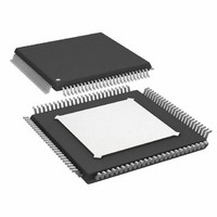
100-TQFP Exposed Pad, 100-eTQFP, 100-HTQFP, 100-VQFP
Lead Free Status / RoHS Status
Lead free / RoHS Compliant
For Use With
AD9272-65EBZ - BOARD EVAL AD9272
Lead Free Status / RoHS Status
Lead free / RoHS Compliant
Available stocks
Company
Part Number
Manufacturer
Quantity
Price
Company:

Part Number:
AD9272BSVZ-80
Manufacturer:
AD
Quantity:
1 001
Company:
Part Number:
AD9272BSVZ-80
Manufacturer:
Analog Devices Inc
Quantity:
135
Company:
Part Number:
AD9272BSVZ-80
Manufacturer:
Analog Devices Inc
Quantity:
10 000


AD9272
The duty cycle stabilizer uses a delay-locked loop (DLL) to
create the nonsampling edge. As a result, any changes to the
sampling frequency require approximately eight clock cycles
to allow the DLL to acquire and lock to the new rate.
Clock Jitter Considerations
High speed, high resolution ADCs are sensitive to the quality of the
clock input. The degradation in SNR at a given input frequency (f
due only to aperture jitter (t
In this equation, the rms aperture jitter represents the root mean
square of all jitter sources, including the clock input, analog input
signal, and ADC aperture jitter. IF undersampling applications
are particularly sensitive to jitter (see Figure 59).
The clock input should be treated as an analog signal in cases
where aperture jitter may affect the dynamic range of the AD9272.
Power supplies for clock drivers should be separated from the
ADC output driver supplies to avoid modulating the clock signal
with digital noise. Low jitter, crystal-controlled oscillators make
the best clock sources, such as the Valpey Fisher VFAC3 series.
If the clock is generated from another type of source (by gating,
dividing, or other methods), it should be retimed by the
original clock during the last step.
Refer to the AN-501 Application Note and the AN-756
Application Note for more in-depth information about how
jitter performance relates to ADCs (visit www.analog.com).
Power Dissipation and Power-Down Mode
As shown in Figure 61, the power dissipated by the AD9272 is
proportional to its sample rate. The digital power dissipation
does not vary much because it is determined primarily by the
DRVDD supply and bias current of the LVDS output drivers.
SNR Degradation = 20 × log 10[1/2 × π × f
130
120
110
100
90
80
70
60
50
40
30
Figure 59. Ideal SNR vs. Analog Input Frequency and Jitter
1
10 BITS
8 BITS
RMS CLOCK JITTER REQUIREMENT
ANALOG INPUT FREQUENCY (MHz)
10
J
) can be calculated by
0.125ps
0.25ps
0.5ps
1.0ps
2.0ps
100
A
× t
16 BITS
14 BITS
12 BITS
J
]
1000
Rev. C | Page 32 of 44
A
)
The AD9272 features scalable LNA bias currents (see Register 0x12
in Table 17). The default LNA bias current settings are high.
Figure 62 shows the typical reduction of AVDD2 current with
each bias setting. It is also recommended to adjust the LNA offset
using Register 0x10 in Table 17 when the LNA bias setting is low.
MID-HIGH
MID-LOW
Figure 62. AVDD2 Current at Different LNA Bias Settings, AD9272-40
400
350
300
250
200
150
100
220
215
210
205
200
195
190
185
180
175
170
HIGH
50
LOW
0
Figure 61. Power per Channel vs. f
0
0
Figure 60. Supply Current vs. f
0
I
AVDD1
10
10
50
, 80MSPS SPEED GRADE
20
20
SAMPLING FREQUENCY (MSPS)
SAMPLING FREQUENCY (MSPS)
80MSPS SPEED GRADE
100
I
AVDD1
TOTAL AVDD2 CURRENT (mA)
30
40MSPS SPEED GRADE
30
, 40MSPS SPEED GRADE
150
I
DRVDD
40
40
I
AVDD1
200
SAMPLE
65MSPS SPEED GRADE
50
SAMPLE
50
, 65MSPS SPEED GRADE
for f
250
for f
60
60
IN
= 5 MHz
IN
= 5 MHz
300
70
70
350
80
80
400
Related parts for AD9272BSVZ-80
Image
Part Number
Description
Manufacturer
Datasheet
Request
R

Part Number:
Description:
±1.7g Dual-Axis IMEMS Accelerometer Evaluation Board
Manufacturer:
Analog Devices Inc
Datasheet:

Part Number:
Description:
Inertial Sensor Evaluation System
Manufacturer:
Analog Devices Inc
Datasheet:
Part Number:
Description:
Manufacturer:
Analog Devices Inc
Datasheet:
Part Number:
Description:
Manufacturer:
Analog Devices Inc
Datasheet:
Part Number:
Description:
Manufacturer:
Analog Devices Inc
Datasheet:
Part Number:
Description:
Manufacturer:
Analog Devices Inc
Datasheet:
Part Number:
Description:
Manufacturer:
Analog Devices Inc
Datasheet:
Part Number:
Description:
Manufacturer:
Analog Devices Inc
Datasheet:
Part Number:
Description:
Manufacturer:
Analog Devices Inc
Datasheet:
Part Number:
Description:
Manufacturer:
Analog Devices Inc
Datasheet:
Part Number:
Description:
Manufacturer:
Analog Devices Inc
Datasheet:
Part Number:
Description:
Manufacturer:
Analog Devices Inc
Datasheet:
Part Number:
Description:
Manufacturer:
Analog Devices Inc
Datasheet: