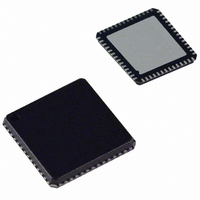
AD9211BCPZ-250 Analog Devices Inc, AD9211BCPZ-250 Datasheet - Page 26

AD9211BCPZ-250
Manufacturer Part Number
AD9211BCPZ-250
Description
IC,A/D CONVERTER,SINGLE,10-BIT,CMOS,LLCC,56PIN
Manufacturer
Analog Devices Inc
Datasheet
1.AD9211BCPZ-200.pdf
(28 pages)
Specifications of AD9211BCPZ-250
Number Of Bits
10
Sampling Rate (per Second)
250M
Data Interface
Serial, SPI™
Number Of Converters
1
Power Dissipation (max)
403mW
Voltage Supply Source
Analog and Digital
Operating Temperature
-40°C ~ 85°C
Mounting Type
Surface Mount
Package / Case
56-LFCSP
Lead Free Status / RoHS Status
Lead free / RoHS Compliant
For Use With
AD9211-300EBZ - BOARD EVALUATION FOR AD9211-300AD9211-250EBZ - BOARD EVAL FOR AD9211-250AD9211-200EBZ - BOARD EVAL FOR AD9211-200
Lead Free Status / RoHS Status
Lead free / RoHS Compliant
Available stocks
Company
Part Number
Manufacturer
Quantity
Price
Part Number:
AD9211BCPZ-250
Manufacturer:
ADI/亚德诺
Quantity:
20 000
AD9211
Addr.
(Hex)
ADC Functions
08
09
OD
OF
14
15
16
Parameter Name
modes
clock
test_io
ain_config
output_mode
output_adjust
output_phase
Bit 7
(MSB)
0
0
0
0
0
Output
clock
polarity
1 =
inverted
0 =
normal
(default)
Bit 6
0
0
0
0
0
Bit 5
PWDN:
0 = full
(default)
1 =
standby
0
Reset
PN23
gen:
1 = on
0 = off
(default)
0
0
0
Bit 4
0
0
Reset
PN9 gen:
1 = on
0 = off
(default)
0
Output
enable:
0 =
enable
(default)
1 =
disable
0
Rev. 0 | Page 26 of 28
Bit 3
0
0
0
DDR:
1 =
enabled
0 =
disabled
(default)
LVDS
course
adjust:
0 =
3.5 mA
(default)
1 =
2.0 mA
(Format determined by output_mode)
0111 = one/zero word toggle
0100 = checker board output
0101 = PN 23 sequence
0001 = midscale short
Bit 2
0
Analog
input
disable:
1 = on
0 = off
(default)
Output
invert:
1 = on
0 = off
(default)
0000 = off (default)
Output test mode:
0010 = +FS short
0011 = −FS short
Internal power-down mode:
1000 = unused
1001 = unused
1010 = unused
1011 = unused
1100 = unused
000 = normal (power-up,
011 = normal (power-up)
Note: External PWDN pin
0110 = PN 9
001 = full power-down
overrides this setting.
LVDS fine adjust:
010 = standby
001 = 3.50 mA
010 = 3.25 mA
011 = 3.00 mA
100 = 2.75 mA
101 = 2.50 mA
110 = 2.25 mA
111 = 2.00 mA
Bit 1
0
CML
enable:
1 = on
0 = off
(default)
default)
Data format select:
00 = offset binary
10 = Gray code
complement
01 = twos
(default)
Bit 0
(LSB)
Duty
cycle
stabilizer:
0 =
disabled
1 =
enabled
(default)
0
Default
Value
(Hex)
0x00
0x01
0x00
0x00
0x00
0x00
0x03
Default Notes/
Comments
Determines
various generic
modes of chip
operation.
When set, the
test data is
placed on the
output pins in
place of normal
data.
0
0


