AD9211-300EBZ Analog Devices Inc, AD9211-300EBZ Datasheet - Page 11
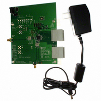
AD9211-300EBZ
Manufacturer Part Number
AD9211-300EBZ
Description
10-Bit 300 Msps ADC
Manufacturer
Analog Devices Inc
Datasheet
1.AD9211BCPZ-200.pdf
(28 pages)
Specifications of AD9211-300EBZ
Number Of Adc's
1
Number Of Bits
10
Sampling Rate (per Second)
300M
Data Interface
Serial
Inputs Per Adc
1 Differential
Input Range
0.98 ~ 1.5 V
Power (typ) @ Conditions
437mW @ 1.8 V
Voltage Supply Source
Analog and Digital
Operating Temperature
-40°C ~ 85°C
Utilized Ic / Part
AD9211
Lead Free Status / RoHS Status
Lead free / RoHS Compliant


Table 8. Double Data Rate Mode Pin Function Descriptions
Pin No.
30, 32 to 34, 37 to 39,
41 to 43, 46
7, 24, 47
0
8, 23, 48
35
36
40
44
45
31
28
25
26
27
29
49
50
53
54
55
56
1
2
3
4
5
6
Mnemonic
AVDD
DRVDD
AGND
DRGND
VIN+
VIN−
CML
CLK+
CLK−
RBIAS
RESET
SDIO/DCS
SCLK/DFS
CSB
PWDN
DCO−
DCO+
D0/D5−
D0/D5+
D1/D6−
D1/D6+
D2/D7−
D2/D7+
D3/D8−
D3/D8+
D4/D9−
D4/D9+
1
1
DNC = DO NOT CONNECT
1.8 V Digital Output Supply.
Clock Input—Complement.
Set Pin for Chip Bias Current. (Place 1% 10 kΩ resistor terminated to ground.) Nominally 0.5 V.
CMOS-Compatible Chip Reset (Active Low).
Chip Power-Down.
(MSB) D4/D9–
(MSB) D4/D9+
Description
1.8 V Analog Supply.
Analog Ground.
Digital Output Ground.
Analog Input—True.
Analog Input—Complement.
Common-Mode Output Pin. Enabled through the SPI, this pin provides a reference for the
optimized internal bias voltage for VIN+/VIN−.
Clock Input—True.
Serial Port Interface (SPI) Data Input/Output (Serial Port Mode); Duty Cycle Stabilizer Select
(External Pin Mode).
Serial Port Interface Clock (Serial Port Mode); Data Format Select Pin (External Pin Mode).
Serial Port Chip Select (Active Low).
Data Clock Output—Complement.
Data Clock Output—True.
D1/D7 Complement Output Bit (LSB).
D1/D7 True Output Bit (LSB).
D2/D8 Complement Output Bit.
D2/D8 True Output Bit.
D3/D9 Complement Output Bit.
D3/D9 True Output Bit.
D4/D10 Complement Output Bit.
D4/D10 True Output Bit.
D5/D11 Complement Output Bit (MSB).
D5/D11 True Output Bit (MSB).
DRGND
DRVDD
D2/D7–
D2/D7+
D3/D8+
D3/D8–
Figure 5. AD9211 Double Data Rate Pin Configuration
OR+
DNC
DNC
DNC
DNC
OR–
10
11
12
13
14
1
2
3
4
5
6
7
8
9
PIN 0 (EXPOSED PADDLE) = AGND
PIN 1
INDICATOR
Rev. 0 | Page 11 of 28
(Not to Scale)
AD9211
TOP VIEW
42 AVDD
41 AVDD
40 CML
39 AVDD
38 AVDD
37 AVDD
36 VIN–
35 VIN+
34 AVDD
33 AVDD
32 AVDD
31 RBIAS
30 AVDD
29 PWDN
AD9211
Related parts for AD9211-300EBZ
Image
Part Number
Description
Manufacturer
Datasheet
Request
R

Part Number:
Description:
10-Bit 200 Msps ADC
Manufacturer:
Analog Devices Inc
Datasheet:
Part Number:
Description:
10-Bit 250 Msps ADC
Manufacturer:
Analog Devices Inc
Datasheet:

Part Number:
Description:
±1.7g Dual-Axis IMEMS Accelerometer Evaluation Board
Manufacturer:
Analog Devices Inc
Datasheet:
Part Number:
Description:
Inertial Sensor Evaluation System
Manufacturer:
Analog Devices Inc
Datasheet:
Part Number:
Description:
Manufacturer:
Analog Devices Inc
Datasheet:
Part Number:
Description:
Manufacturer:
Analog Devices Inc
Datasheet:
Part Number:
Description:
Manufacturer:
Analog Devices Inc
Datasheet:
Part Number:
Description:
Manufacturer:
Analog Devices Inc
Datasheet:
Part Number:
Description:
Manufacturer:
Analog Devices Inc
Datasheet:
Part Number:
Description:
Manufacturer:
Analog Devices Inc
Datasheet:
Part Number:
Description:
Manufacturer:
Analog Devices Inc
Datasheet:
Part Number:
Description:
Manufacturer:
Analog Devices Inc
Datasheet:
Part Number:
Description:
Manufacturer:
Analog Devices Inc
Datasheet: