AD8367ARUZ-RL7 Analog Devices Inc, AD8367ARUZ-RL7 Datasheet - Page 6
AD8367ARUZ-RL7
Manufacturer Part Number
AD8367ARUZ-RL7
Description
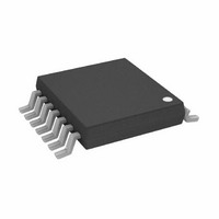
IC,Voltage Controlled Gain Amplifier,SINGLE,TSSOP,14PIN,PLASTIC
Manufacturer
Analog Devices Inc
Series
X-AMP®r
Type
Variable Gain Amplifierr
Datasheet
1.AD8367-EVAL.pdf
(24 pages)
Specifications of AD8367ARUZ-RL7
Amplifier Type
Variable Gain
Number Of Circuits
1
-3db Bandwidth
500MHz
Current - Input Bias
27µA
Current - Supply
26mA
Voltage - Supply, Single/dual (±)
2.7 V ~ 5.5 V
Operating Temperature
-40°C ~ 85°C
Mounting Type
Surface Mount
Package / Case
14-TSSOP
Number Of Channels
1
Number Of Elements
1
Power Supply Requirement
Single
Voltage Gain Db
45dB
Input Resistance
0.000225@5VMohm
Input Bias Current
27@5VnA
Single Supply Voltage (typ)
3/5V
Dual Supply Voltage (typ)
Not RequiredV
Power Dissipation
250mW
Rail/rail I/o Type
No
Single Supply Voltage (min)
2.7V
Single Supply Voltage (max)
5.5V
Dual Supply Voltage (min)
Not RequiredV
Dual Supply Voltage (max)
Not RequiredV
Operating Temp Range
-40C to 85C
Operating Temperature Classification
Industrial
Mounting
Surface Mount
Pin Count
14
Package Type
TSSOP
Lead Free Status / RoHS Status
Lead free / RoHS Compliant
Output Type
-
Current - Output / Channel
-
Slew Rate
-
Gain Bandwidth Product
-
Voltage - Input Offset
-
Lead Free Status / Rohs Status
Compliant
Available stocks
Company
Part Number
Manufacturer
Quantity
Price

Part Number:
AD8367ARUZ-RL7
Manufacturer:
ADI/亚德诺
Quantity:
20 000


AD8367
PIN CONFIGURATION AND FUNCTION DESCRIPTIONS
Table 3. Pin Function Descriptions
Pin No.
1, 7, 14
2
3
4
5
6
8
9
10
11
12
13
Mnemonic
ICOM
ENBL
INPT
MODE
GAIN
DETO
OCOM
DECL
VOUT
VPSO
VPSI
HPFL
Description
Signal Common. Connect to low impedance ground.
A HI Activates the Device.
Signal Input. 200 Ω to ground.
Gain Direction Control. HI for positive slope; LO for negative slope.
Gain Control Voltage Input.
Detector Output. Provides output current for RSSI function and AGC control.
Power Common. Connect to low impedance ground.
Output Centering Loop Decoupling Pin.
Signal Output. To be externally ac-coupled to load.
Positive Supply Voltage. 2.7 V to 5.5 V. VPSI and VPSO are tied together internally with back-to-back
PN junctions. They should be tied together externally and properly bypassed.
Positive Supply Voltage. 2.7 V to 5.5 V.
High-Pass Filter Connection. A capacitor to ground sets the corner frequency of the output offset control loop.
MODE
DETO
ENBL
ICOM
ICOM
GAIN
INPT
Figure 2. Pin Configuration
1
2
3
4
5
6
7
Rev. A | Page 6 of 24
(Not to Scale)
AD8367
TOP VIEW
14
13
12
11
10
9
8
ICOM
HPFL
VPSI
VPSO
VOUT
DECL
OCOM
Related parts for AD8367ARUZ-RL7
Image
Part Number
Description
Manufacturer
Datasheet
Request
R

Part Number:
Description:
Amplifier IC
Manufacturer:
Analog Devices Inc
Datasheet:
Part Number:
Description:
IC,Voltage Controlled Gain Amplifier,SINGLE,TSSOP,14PIN,PLASTIC
Manufacturer:
Analog Devices Inc
Datasheet:

Part Number:
Description:
BOARD EVAL FOR AD8367
Manufacturer:
Analog Devices Inc
Datasheet:

Part Number:
Description:
500 MHz, Linear-in-dB VGA with AGC Detector
Manufacturer:
Analog Devices
Datasheet:

Part Number:
Description:
±1.7g Dual-Axis IMEMS Accelerometer Evaluation Board
Manufacturer:
Analog Devices Inc
Datasheet:
Part Number:
Description:
Inertial Sensor Evaluation System
Manufacturer:
Analog Devices Inc
Datasheet:
Part Number:
Description:
Manufacturer:
Analog Devices Inc
Datasheet:
Part Number:
Description:
Manufacturer:
Analog Devices Inc
Datasheet:
Part Number:
Description:
Manufacturer:
Analog Devices Inc
Datasheet:
Part Number:
Description:
Manufacturer:
Analog Devices Inc
Datasheet:
Part Number:
Description:
Manufacturer:
Analog Devices Inc
Datasheet:
Part Number:
Description:
Manufacturer:
Analog Devices Inc
Datasheet:
Part Number:
Description:
Manufacturer:
Analog Devices Inc
Datasheet: