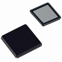
AD8190ACPZ-R7 Analog Devices Inc, AD8190ACPZ-R7 Datasheet - Page 5

AD8190ACPZ-R7
Manufacturer Part Number
AD8190ACPZ-R7
Description
IC,Telecom Switching Circuit,LLCC,56PIN,PLASTIC
Manufacturer
Analog Devices Inc
Datasheet
1.AD8190ACPZ-R7.pdf
(24 pages)
Specifications of AD8190ACPZ-R7
Applications
*
Mounting Type
Surface Mount
Package / Case
56-LFCSP
Lead Free Status / RoHS Status
Lead free / RoHS Compliant
For Use With
AD8190-9880/PCB - KIT EVAL FOR AD8190 & AD9880
Lead Free Status / RoHS Status
Lead free / RoHS Compliant
Available stocks
Company
Part Number
Manufacturer
Quantity
Price
Part Number:
AD8190ACPZ-R7
Manufacturer:
ADI/亚德诺
Quantity:
20 000
ABSOLUTE MAXIMUM RATINGS
Table 2.
Parameter
AVCC to AVEE
DVCC to DVEE
DVEE to AVEE
VTTI
VTTO
AMUXVCC
Internal Power Dissipation
High Speed Input Voltage
High Speed Differential
Input Voltage
Low Speed Input Voltage
I
Storage Temperature
Range
Operating Temperature
Range
Junction Temperature
Stresses above those listed under Absolute Maximum Ratings
may cause permanent damage to the device. This is a stress
rating only; functional operation of the device at these or any
other conditions above those indicated in the operational
section of this specification is not implied. Exposure to absolute
maximum rating conditions for extended periods may affect
device reliability.
ESD CAUTION
ESD (electrostatic discharge) sensitive device. Electrostatic charges as high as 4000 V readily accumulate on
the human body and test equipment and can discharge without detection. Although this product features
proprietary ESD protection circuitry, permanent damage may occur on devices subjected to high energy
electrostatic discharges. Therefore, proper ESD precautions are recommended to avoid performance
degradation or loss of functionality.
2
C Logic Input Voltage
Rating
3.7 V
3.7 V
±0.3 V
AVCC + 0.6 V
AVCC + 0.6 V
5.5 V
AVCC − 1.4 V < V
2.0 V
DVEE − 0.3 V < V
DVEE − 0.3 V < V
−65°C to +125°C
−40°C to +85°C
150°C
4.62 W
IN
IN
IN
< AMUXVCC + 0.6 V
< DVCC + 0.6 V
< AVCC + 0.6 V
Rev. 0 | Page 5 of 24
THERMAL RESISTANCE
θ
in a 4-layer JEDEC circuit board for surface-mount packages.
θ
with no airflow.
Table 3. Thermal Resistance
Package Type
56-Lead LFCSP
MAXIMUM POWER DISSIPATION
The maximum power that can be safely dissipated by the
AD8190 is limited by the associated rise in junction tempera-
ture. The maximum safe junction temperature for plastic
encapsulated devices is determined by the glass transition
temperature of the plastic, approximately 150°C. Temporarily
exceeding this limit may cause a shift in parametric performance
due to a change in the stresses exerted on the die by the package.
Exceeding a junction temperature of 175°C for an extended
period can result in device failure. To ensure proper operation,
it is necessary to observe the maximum power derating as
determined by the coefficients in Table 3.
JA
JC
is specified for the worst-case conditions: a device soldered
is specified for the exposed pad soldered to the circuit board
θ
27
JA
θ
2.1
JC
AD8190
Unit
°C/W


