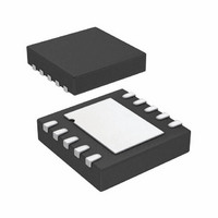
AD7983BCPZ-RL Analog Devices Inc, AD7983BCPZ-RL Datasheet - Page 21

AD7983BCPZ-RL
Manufacturer Part Number
AD7983BCPZ-RL
Description
IC,A/D CONVERTER,SINGLE,16-BIT,LLCC,10PIN
Manufacturer
Analog Devices Inc
Series
PulSAR®r
Datasheet
1.AD7983BRMZ.pdf
(24 pages)
Specifications of AD7983BCPZ-RL
Number Of Bits
16
Sampling Rate (per Second)
1.33M
Data Interface
DSP, MICROWIRE™, QSPI™, Serial, SPI™
Number Of Converters
1
Power Dissipation (max)
12mW
Voltage Supply Source
Single Supply
Operating Temperature
-40°C ~ 85°C
Mounting Type
Surface Mount
Package / Case
10-WFDFN, CSP Exposed Pad
Lead Free Status / RoHS Status
Lead free / RoHS Compliant
Available stocks
Company
Part Number
Manufacturer
Quantity
Price
Part Number:
AD7983BCPZ-RL7
Manufacturer:
ADI/亚德诺
Quantity:
20 000
CHAIN MODE WITHOUT BUSY INDICATOR
This mode can be used to daisy-chain multiple AD7983s on a
3-wire serial interface. This feature is useful for reducing
component count and wiring connections, for example, in
isolated multiconverter applications or for systems with a
limited interfacing capacity. Data readback is analogous to
clocking a shift register.
A connection diagram example using two AD7983s is shown in
Figure 34, and the corresponding timing is given in Figure 35.
ACQUISITION
SDO
A
SDI
= SDI
SDO
A
t
CNV
SCK
HSCKCNV
= 0
B
B
CONVERSION
t
SSCKCNV
t
CONV
t
EN
SDI
AD7983
t
CNV
SCK
HSDO
Figure 35. Chain Mode Without Busy Indicator Serial Interface Timing
A
Figure 34. Chain Mode Without Busy Indicator Connection Diagram
D
D
A
B
15
15
1
SDO
t
SSDISCK
D
D
2
A
B
14
14
t
DSDO
D
D
3
A
B
13
13
Rev. A | Page 21 of 24
t
SCKL
SDI
t
HSDISCK
14
AD7983
CNV
SCK
B
t
D
D
15
CYC
When SDI and CNV are low, SDO is driven low. With SCK low,
a rising edge on CNV initiates a conversion, selects the chain
mode, and disables the busy indicator. In this mode, CNV is
held high during the conversion phase and the subsequent data
readback. When the conversion is complete, the MSB is output
onto SDO and the AD7983 enters the acquisition phase and
goes into standby mode. The remaining data bits stored in the
internal shift register are clocked by subsequent SCK falling
edges. For each ADC, SDI feeds the input of the internal shift
register and is clocked by the SCK falling edge. Each ADC in
the chain outputs its data MSB first, and 16 × N clocks are
required to readback the N ADCs. The data is valid on both
SCK edges. Although the rising edge can be used to capture the
data, a digital host using the SCK falling edge allows a faster
reading rate and, consequently, more AD7983s in the chain,
provided the digital host has an acceptable hold time. The
maximum conversion rate can be reduced due to the total
readback time.
A
B
1
1
ACQUISITION
t
SCK
SDO
t
t
SCKH
D
D
16
ACQ
A
B
0
0
D
17
A
15
CONVERT
DATA IN
CLK
D
DIGITAL HOST
18
A
14
30
D
31
A
1
D
32
A
0
AD7983


