AD7898AR-10REEL7 Analog Devices Inc, AD7898AR-10REEL7 Datasheet
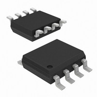
IC,A/D CONVERTER,SINGLE,12-BIT,SOP,8PIN

AD7898AR-10REEL7

Manufacturer Part Number
AD7898AR-10REEL7
Description
IC,A/D CONVERTER,SINGLE,12-BIT,SOP,8PIN
Manufacturer
Analog Devices Inc
Datasheet

Specifications of AD7898AR-10REEL7

Rohs Status
RoHS non-compliant
Number Of Bits
12
Sampling Rate (per Second)
220k
Data Interface
Serial
Number Of Converters
1
Power Dissipation (max)
22.5mW
Voltage Supply Source
Single Supply
Operating Temperature
-40°C ~ 85°C
Mounting Type
Surface Mount
Package / Case
8-SOIC (0.154", 3.90mm Width)
Lead Free Status / RoHS Status
a
GENERAL DESCRIPTION
The AD7898 is a fast 12-bit ADC that operates from a single
5 V supply and is housed in a small 8-lead SOIC package. The
part contains a successive approximation A/D converter, an on-
chip track/hold amplifier, an on-chip clock, and a high speed
serial interface.
The AD7898 offers two modes of operation. In Mode 0, con-
version is initiated by the CONVST input and the conversion
process is controlled by an internal clock oscillator. In this mode,
the serial interface consists of three wires and the AD7898 is
capable of throughput rates up to 220 kSPS. In Mode 1, the
conversion process is controlled by an externally applied SCLK
with data being accessed from the part during conversion. In
this mode, the serial interface consists of three wires and the
AD7898 is capable of throughput rates up to 220 kSPS.
In addition to the traditional dc accuracy specifications, such as
linearity and full-scale and offset errors, the AD7898 is specified
for dynamic performance parameters, including harmonic dis-
tortion and signal-to-noise ratio.
The part accepts an analog input range of ± 10 V (AD7898-10)
and ± 2.5 V (AD7898-3), and operates from a single 5 V supply,
consuming only 22.5 mW max.
The part is available in an 8-lead Standard Small Outline
Package (SOIC).
*Protected by U.S. Patent No. 6,681,332
REV. A
Information furnished by Analog Devices is believed to be accurate and
reliable. However, no responsibility is assumed by Analog Devices for its
use, nor for any infringements of patents or other rights of third parties that
may result from its use. No license is granted by implication or otherwise
under any patent or patent rights of Analog Devices. Trademarks and
registered trademarks are the property of their respective owners.
FEATURES
Fast 12-Bit ADC with 220 kSPS Throughput Rate
8-Lead SOIC
Single 5 V Supply Operation
High Speed, Flexible, Serial Interface that
On-Chip Track/Hold Amplifier
Selection of Input Ranges
High Input Impedance
Low Power: 22.5 mW Max
Allows Interfacing to 3 V Processors
10 V for AD7898-10
2.5 V for AD7898-3
One Technology Way, P.O. Box 9106, Norwood, MA 02062-9106, U.S.A.
Tel: 781/329-4700
Fax: 781/326-8703
PRODUCT HIGHLIGHTS
1. Fast, 12-Bit ADC in 8-Lead Package
2. Low Power, Single-Supply Operation
3. Flexible, High Speed Serial Interface
4. Power-Down Mode
The AD7898 contains a 220 kSPS ADC, a track/hold ampli-
fier, control logic, and a high speed serial interface, all in an
8-lead package. This offers considerable space saving over
alternative solutions.
The AD7898 operates from a single 5 V supply and con-
sumes only 22.5 mW. The V
interface to connect directly to either 3 V or 5 V processor
systems independent of V
The part provides a flexible, high speed serial interface that
has two distinct modes of operation. Mode 0 provides a three-
wire interface with data being accessed from the AD7898
when conversion is complete. Mode 1 offers a three-wire
interface with data being accessed during conversion.
The AD7898 offers a proprietary power-down capability
when operated in Mode 1, making the part ideal for portable
or hand-held applications.
5 V, 12-Bit, Serial 220 kSPS
CONVST
ADC in an 8-Lead Package
FUNCTIONAL BLOCK DIAGRAM
V
IN
*AD7898-10, AD7898-3
© 2004 Analog Devices, Inc. All rights reserved.
SCALING*
AD7898
SIGNAL
GND
DD
TRACK/HOLD
VDRIVE
.
DRIVE
REF IN
function allows the serial
AD7898
SCLK
REGISTER
OUTPUT
12-BIT
ADC
www.analog.com
V
SDATA
DD
*

Related parts for AD7898AR-10REEL7

AD7898AR-10REEL7 Summary of contents

Page 1

FEATURES Fast 12-Bit ADC with 220 kSPS Throughput Rate 8-Lead SOIC Single 5 V Supply Operation High Speed, Flexible, Serial Interface that Allows Interfacing Processors On-Chip Track/Hold Amplifier Selection of Input Ranges 10 V for AD7898-10 ...

Page 2

AD7898–SPECIFICATIONS Parameter DYNAMIC PERFORMANCE 2 Signal to (Noise + Distortion) Ratio MIN MAX 2 Total Harmonic Distortion (THD) 2 Peak Harmonic or Spurious Noise 2 Intermodulation Distortion (IMD) 2nd Order Terms 3rd Order Terms Aperture Delay Aperture ...

Page 3

TIMING SPECIFICATIONS Parameter Limit MIN MAX Mode 0 Operation ...

Page 4

... This is a stress rating; functional operation of the device at these or any other conditions above those listed in the operational sections of this specification is not implied. Exposure to absolute maximum rating conditions for extended periods may affect device reliability. Model AD7898AR-10 AD7898AR-10REEL AD7898AR-10REEL7 3 AD7898ARZ-10 3 AD7898ARZ-10REEL 3 AD7898ARZ-10REEL7 ...

Page 5

Pin Pin No. Mnemonic Function 1 REF IN Voltage Reference Input. An external reference source should be connected to this pin to provide the reference voltage for the AD7898’s conversion process. The REF IN input is buffered on-chip. The nominal ...

Page 6

AD7898 TERMINOLOGY Signal to (Noise + Distortion) Ratio This is the measured ratio of signal to (noise + distortion) at the output of the A/D converter. The signal is the rms amplitude of the fundamental. Noise is the rms sum ...

Page 7

PERFORMANCE CURVES TPC 1 shows a typical FFT plot for the AD7898 at 220 kSPS sampling rate with a 30 kHz input frequency while operating in Mode 0. 5 –15 –35 –55 –75 –95 –115 FREQUENCY ...

Page 8

AD7898 –40 –45 –50 –55 – – 4.75V DD DRIVE – 5.0V –75 10 100 INPUT FREQUENCY – kHz TPC 5. SINAD vs. Input Frequency at 220 kSPS TPC 5 ...

Page 9

Figure 2 shows the analog input section for the AD7898-10 and AD7898-3. The analog input range of the AD7898-10 is ± into an input resistance of typically 30 kΩ. The analog input range of the AD7898-3 is ± ...

Page 10

AD7898 TYPICAL CONNECTION DIAGRAM Figure 5 shows a typical connection diagram for the AD7898. The GND pin is connected to the analog ground plane of the system. REF IN is connected to a decoupled 2.5 V supply from a reference ...

Page 11

CONVST SCLK CONVERSION IS INITIATED AND TRACK/HOLD GOES INTO HOLD t SCLK 1 2 SDATA Z ZERO THREE-STATE FOUR LEADING ZEROS Figure 7 shows the timing diagram for the read operation to the AD7898 in Mode 0. The ...

Page 12

AD7898 SCLK SDATA Z ZERO ZERO THREE-STATE FOUR LEADING ZEROS Mode 1 Operation The timing diagram in Figure 8 shows the AD7898 operating in Mode 1. The serial clock provides the conversion clock ...

Page 13

CS SCLK SDATA THE PART BEGINS TO POWER SCLK SDATA To enter power-down, the conversion process must be inter- rupted by bringing CS high anywhere after the fourth falling edge of SCLK and before the 11th falling ...

Page 14

AD7898 To chip-select the AD7898 in systems where more than one device is connected to the 8x51/L51’s serial port, a port bit configured as an output, from one of the 8x51/L51’s parallel ports can be used to gate on or ...

Page 15

TMS320C5x/C54x to AD7898 Interface The serial interface on the TMS320C5x/C54x uses a continu- ous serial clock and frame synchronization signal to synchronize the data transfer operations with peripheral devices like the AD7898. The CS input allows easy interfacing between the ...

Page 16

AD7898 AD7898 to MC68HC16 Interface The Serial Peripheral Interface (SPI) on the MC68HC16 is configured for Master Mode (MSTR = 1), Clock Polarity Bit (CPOL and the Clock Phase Bit (CPHA The SPI is configured by ...

Related keywords