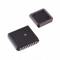
AD7891AP-2 Analog Devices Inc, AD7891AP-2 Datasheet - Page 7

AD7891AP-2
Manufacturer Part Number
AD7891AP-2
Description
A/D Converter (A-D) IC
Manufacturer
Analog Devices Inc
Type
Data Acquisition System (DAS)r
Datasheet
1.AD7891BSZ-2.pdf
(20 pages)
Specifications of AD7891AP-2
No. Of Bits
12 Bit
Mounting Type
Surface Mount
Features
8?Ch., High?Speed, Data Acquisition System
No. Of Channels
8
Interface Type
Parallel
Package / Case
44-PLCC
Rohs Status
RoHS non-compliant
Resolution (bits)
12 b
Sampling Rate (per Second)
500k
Data Interface
Serial, Parallel
Voltage Supply Source
Single Supply
Voltage - Supply
5V
Operating Temperature
-40°C ~ 85°C
Lead Free Status / RoHS Status
Available stocks
Company
Part Number
Manufacturer
Quantity
Price
Company:
Part Number:
AD7891AP-2
Manufacturer:
Analog Devices Inc
Quantity:
10 000
Part Number:
AD7891AP-2
Manufacturer:
ADI/亚德诺
Quantity:
20 000
Company:
Part Number:
AD7891AP-2REEL
Manufacturer:
Analog Devices Inc
Quantity:
10 000
PLCC Pin No. MQFP Pin No. Mnemonic
8, 31
29
28
27
Data I/O Lines
There are 12 data input/output lines on the AD7891. When the part is configured for parallel mode (MODE = 1), the output data
from the part is provided at these 12 pins during a read operation. For a write operation in parallel mode, these lines provide access
to the part’s control register.
Parallel Read Operation
During a parallel read operation, the 12 lines become the 12 data bits containing the conversion result from the AD7891. These
data bits are labelled Data Bit 0 (LSB) to Data Bit 11 (MSB). They are three-state, TTL compatible outputs. Output data coding
is twos complement when the data FORMAT bit of the control register is 1, and straight binary when the data FORMAT bit of
the control register is 0.
PLCC Pin No. MQFP Pin No. Mnemonic
13 to 18,
21 to 26
Parallel Write Operation
During a parallel write operation, the following functions can be written to the control register via the 12 data input/output pins.
PLCC Pin No. MQFP Pin No. Mnemonic
23
22
21
24
25
26
REV. D
2, 25
23
22
21
7 to 12,
15 to 20
17
16
15
18
19
20
NC
CS
RD
WR
DB0 to DB11 Data Bit 0 (LSB) to Data Bit 11 (MSB). Three-state TTL compatible
A0
A1
A2
SWCON
SWSTBY
FORMAT
PARALLEL INTERFACE MODE FUNCTIONS
Description
No Connect. The two NC pins on the device can be left unconnected. If they
are to be connected to a voltage, it should be to ground potential. To ensure
correct operation of the AD7891, neither of the NC pins should be connected
to a logic high potential.
Chip Select Input. Active low logic input that is used in conjunction with to
enable the data outputs and with WR to allow input data to be written to the part.
Read Input. Active low logic input that is used in conjunction with CS low to
enable the data outputs.
Write Input. Active low logic input used in conjunction with CS to latch the mul-
tiplexer address and software control information. The rising edge of this input
also initiates an internal pulse. When using the software start facility, this pulse
delays the point at which the track/hold goes into hold and conversion is initiated.
This allows the multiplexer to settle and the acquisition time of the track/hold to
elapse when a channel address is changed. If the SWCON bit of the control regis-
ter is set to 1, when this pulse times out, the track/hold then goes into hold and
conversion is initiated. If the SWCON bit of the control register is set to 0, the
track/hold and conversion sequence are unaffected by WR operation.
Description
outputs that are controlled by the CS and RD inputs.
Description
Address Input. The status of this input during a parallel write operation is
latched to the A0 bit of the control register (see Control Register section).
Address Input. The status of this input during a parallel write operation is
latched to the A1 bit of the control register (see Control Register section).
Address Input. The status of this input during a parallel write operation is
latched to the A2 bit of the control register (see Control Register section).
Software Conversion Start. The status of this input during a parallel write
operation is latched to the SWCONV bit of the control register (see Control
Register section).
Software Standby Control. The status of this input during a parallel write
operation is latched to the SWSTBY bit of the control register (see Control
Register section).
Data Format Selection. The status of this input during a parallel write operation is
latched to the FORMAT bit of the control register (see Control Register section).
–7–
AD7891


