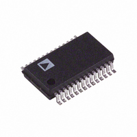
AD7863ARSZ-2 Analog Devices Inc, AD7863ARSZ-2 Datasheet - Page 18

AD7863ARSZ-2
Manufacturer Part Number
AD7863ARSZ-2
Description
IC,Data Acquisition System,2-CHANNEL,14-BIT,SSOP,28PIN,PLASTIC
Manufacturer
Analog Devices Inc
Datasheet
1.AD7863ARZ-3.pdf
(24 pages)
Specifications of AD7863ARSZ-2
Number Of Bits
14
Sampling Rate (per Second)
175k
Data Interface
Parallel
Number Of Converters
2
Power Dissipation (max)
94.5mW
Voltage Supply Source
Analog and Digital
Operating Temperature
-40°C ~ 85°C
Mounting Type
Surface Mount
Package / Case
28-SSOP (0.200", 5.30mm Width)
Lead Free Status / RoHS Status
Lead free / RoHS Compliant
Available stocks
Company
Part Number
Manufacturer
Quantity
Price
Part Number:
AD7863ARSZ-2
Manufacturer:
ADI/亚德诺
Quantity:
20 000
AD7863
Some applications may require that the conversion be initiated
by the microprocessor rather than an external timer. One
option is to decode the AD7863 CONVST from the address bus
so that a write operation starts a conversion. Data is read at the
end of the conversion sequence as before. Figure 23 shows an
example of initiating conversion using this method. Note that
for all interfaces, it is preferred that a read operation not be
attempted during conversion.
AD7863 TO MC68000 INTERFACE
An interface between the AD7863 and the MC68000 is shown
in Figure 22. As before, conversion can be supplied from the
MC68000 or from an external source. The AD7863 BUSY line
can be used to interrupt the processor or, alternatively, software
delays can ensure that conversion has been completed before a
read to the AD7863 is attempted. Because of the nature of its
interrupts, the MC68000 requires additional logic (not shown
in Figure 23) to allow it to be interrupted correctly. For further
information on MC68000 interrupts, consult the MC68000
users manual.
The MC68000 AS and R/ W outputs are used to generate a
separate RD input signal for the AD7863. CS is used to drive
the MC68000 DTACK input to allow the processor to execute
a normal read operation to the AD7863. The conversion results
are read using the following MC68000 instruction:
where:
D0 is the 68000 D0 register.
ADC is the AD7863 address.
MOVE.W ADC, D0
TMS320C25
READY
DMD15
Figure 21. AD7863 to TMS320C25 Interface
DMD0
STRB
INTn
MSC
R/W
A15
A0
IS
*ADDITIONAL PINS OMITTED FOR CLARITY.
EN
ADDRESS BUS
DATA BUS
ADDRESS
DECODE
CS
A0
BUSY
RD
DB13
DB0
OPTIONAL
AD7863*
CONVST
Rev. B | Page 18 of 24
AD7863 TO 80C196 INTERFACE
Figure 23 shows an interface between the AD7863 and the
80C196 microprocessor. Here, the microprocessor initiates
conversion. This is achieved by gating the 80C196 WR signal
with a decoded address output (different from the AD7863 CS
address). The AD7863 BUSY line is used to interrupt the
microprocessor when the conversion sequence is completed.
VECTOR MOTOR CONTROL
The current drawn by a motor can be split into two components:
one produces torque and the other produces magnetic flux.
For optimal performance of the motor, these two components
should be controlled independently. In conventional methods of
controlling a three-phase motor, the current (or voltage)
supplied to the motor and the frequency of the drive are the
basic control variables. However, both the torque and flux are
functions of current (or voltage) and frequency. This coupling
effect can reduce the performance of the motor because, for
example, if the torque is increased by increasing the frequency,
the flux tends to decrease.
MC68000
80C196
DTACK
R/W
A15
D15
A15
D15
WR
RD
AS
A0
D0
A1
D0
Figure 22. AD7863 to MC68000 Interface
Figure 23. AD7863–80C196 Interface
*ADDITIONAL PINS OMITTED FOR CLARITY.
*ADDITIONAL PINS OMITTED FOR CLARITY.
ADDRESS BUS
ADDRESS BUS
ADDRESS
ADDRESS
EN
DATA BUS
EN
DATA BUS
DECODE
DECODE
A0
CS
RD
DB13
DB0
CS
A0
BUSY
DB13
DB0
RD
AD7863*
AD7863*
OPTIONAL
CONVST


