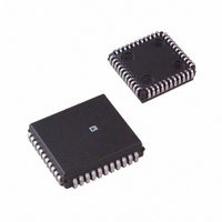
AD7716BPZ Analog Devices Inc, AD7716BPZ Datasheet - Page 11

AD7716BPZ
Manufacturer Part Number
AD7716BPZ
Description
4-CHNL S-D ADC
Manufacturer
Analog Devices Inc
Datasheet
1.AD7716BP-REEL.pdf
(16 pages)
Specifications of AD7716BPZ
Number Of Bits
22
Sampling Rate (per Second)
2.23k
Data Interface
Serial
Number Of Converters
4
Power Dissipation (max)
50mW
Voltage Supply Source
Analog and Digital, Dual ±
Operating Temperature
-40°C ~ 85°C
Mounting Type
Surface Mount
Package / Case
44-PLCC
Lead Free Status / RoHS Status
Lead free / RoHS Compliant
For Use With
EVAL-AD7716EBZ - BOARD EVAL FOR AD7716
Lead Free Status / RoHS Status
Lead free / RoHS Compliant
Available stocks
Company
Part Number
Manufacturer
Quantity
Price
Company:
Part Number:
AD7716BPZ
Manufacturer:
ST
Quantity:
2 100
Company:
Part Number:
AD7716BPZ
Manufacturer:
Analog Devices Inc
Quantity:
10 000
Source Resistance
If passive attenuators are used in front of the AD7716, care
must be taken to ensure that the source impedance is suffi-
ciently low. The dc input resistance for the AD7716 is greater
than 1 G . In parallel with this there is a small sampling ca-
pacitor. The dynamic load presented by this varies with the
clock frequency. The modulator sampling rate determines the
amount of time available for the sampling capacitor to be
charged. Any extra external impedances result in a longer over-
all charge time resulting in extra gain errors on the analog input.
The AD7716 has a quite large gain error (1% FSR) due to the
fact that there is no on-chip calibration. Thus, even an extra
10 k source resistance and 50 pF source capacitance will have
no significant effect on this.
Active signal conditioning circuits such as op amps generally do
not suffer from problems of high source impedance. Their
open-loop output resistance is normally only tens of ohms and,
in any case, most modern general purpose op amps have
sufficiently fast closed-loop settling time for this not to be a
problem.
Accuracy
Sigma-delta ADCs, like VFCs and other integrating ADCs, do
not contain any source of nonmonotonicity and inherently offer
no missing codes performance.
The AD7716 achieves excellent linearity by the use of high
quality, on-chip silicon dioxide capacitors, which have a very
low capacitance/voltage coefficient.
Drift Considerations
The AD7716 uses autozeroing techniques to minimize input
offset drift. Charge injection in the analog switches and leakage
currents at the sampling node are the primary sources of offset
voltage drift in the converter. Figure 7 indicates the typical off-
set due to temperature changes. Drift is relatively flat up to
85 C. Above this temperature, leakage current becomes the
main source of offset drift. Since leakage current doubles ap-
proximately every 10 C, the offset drifts accordingly. The value
of the voltage on the sample capacitor is updated at a rate deter-
mined by the master clock, therefore the amount of offset drift
which occurs will be proportional to the elapsed time between
samples.
Gain drift within the converter depends mainly upon the tem-
perature tracking of the internal capacitors. It is not affected by
leakage currents.
REV. A
–11–
Voltage Reference
The voltage applied to the V
range. The specified reference voltage is 2.5 V
The reference input presents exactly the same dynamic load as
the analog input, but in the case of the reference input, source
resistance and long settling time introduce gain errors rather
than offset errors. Most precision references however have suffi-
ciently low output impedance and wide enough bandwidth to
settle to the required accuracy in the time allowed by the
AD7716.
The reference should be chosen to have minimal noise in the
programmed passband. Recommended references are the
AD780 or the REF43 from Analog Devices. These low noise
references have typical noise spectral densities of 100 nV/ Hz at
600 Hz. This corresponds to an rms noise of 2.5 V in this
band and is more than adequate for the AD7716.
Clock Generation
The device operates from a master clock which must be pro-
vided either from a crystal source or an external clock source. If
a crystal is used, it must be connected across the CLKIN and
CLKOUT pins. Typical loading capacitors of 15 pF are re-
quired on CLKIN, CLKOUT. The crystal manufacturers data
should be consulted for more information. An external clock
can also be used to drive the CLKIN input directly with a
CMOS compatible clock. In this case, CLKOUT is left uncon-
nected. The nominal clock frequency for the device is 8 MHz.
–0.125
–0.375
–0.500
–0.625
–0.25
20
Figure 7. Typical Offset Drift
30
40
TEMPERATURE – C
REF
50
pin defines the analog input
60
70
AD7716
10%.
80
90


