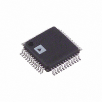
AD7674ASTZRL Analog Devices Inc, AD7674ASTZRL Datasheet - Page 7

AD7674ASTZRL
Manufacturer Part Number
AD7674ASTZRL
Description
IC,A/D CONVERTER,SINGLE,18-BIT,CMOS,QFP,48PIN
Manufacturer
Analog Devices Inc
Series
PulSAR®r
Datasheet
1.AD7674ASTZ.pdf
(28 pages)
Specifications of AD7674ASTZRL
Number Of Bits
18
Sampling Rate (per Second)
800k
Data Interface
Serial, Parallel
Number Of Converters
1
Power Dissipation (max)
138mW
Voltage Supply Source
Analog and Digital
Operating Temperature
-40°C ~ 85°C
Mounting Type
Surface Mount
Package / Case
48-LQFP
Lead Free Status / RoHS Status
Lead free / RoHS Compliant
For Use With
EVAL-AD7674CBZ - BOARD EVALUATION FOR AD7674
Lead Free Status / RoHS Status
Lead free / RoHS Compliant
Available stocks
Company
Part Number
Manufacturer
Quantity
Price
Company:
Part Number:
AD7674ASTZRL
Manufacturer:
Analog Devices Inc
Quantity:
10 000
ABSOLUTE MAXIMUM RATINGS
Table 5. AD7674 Absolute Maximum Ratings
Parameter
Analog Inputs
Ground Voltage Differences
Supply Voltages
Internal Power Dissipation
Internal Power Dissipation
Junction Temperature
Storage Temperature Range
Lead Temperature Range
1
2
3
4
Stresses above those listed under Absolute Maximum Ratings may cause
See Analog Input section.
Specification is for device in free air: 48-Lead LQFP: θ
permanent damage to the device. This is a stress rating only; functional
operation of the device at these or any other conditions above those
indicated in the operational section of this specification is not implied.
Exposure to absolute maximum rating conditions for extended periods may
affect device reliability.
θ
Specification is for device in free air: 48-Lead LFCSP: θ
JC
IN+
AGND, DGND, OGND
AVDD, DVDD, OVDD
AVDD to DVDD, AVDD to OVDD
DVDD to OVDD
Digital Inputs
(Soldering 10 sec)
= 30°C/W.
REFGND to AGND
2
, IN–
2
, REF, REFBUFIN,
3
4
Rating
AGND – 0.3 V to
AVDD + 0.3 V
±0.3 V
–0.3 V to +7 V
±7 V
–0.3 V to +7 V
–0.3 V to DVDD + 0.3 V
700 mW
2.5 W
150°C
–65°C to +150°C
300°C
JA
JA
= 91°C/W,
= 26°C/W.
1
Rev. A | Page 7 of 28
ESD CAUTION
Figure 2. Load Circuit for Digital Interface Timing, SDOUT, SYNC, SCLK
TO OUTPUT
NOTE
1
t
DELAY
IN SERIAL INTERFACE MODES,THE SYNC, SCLK, AND
SDOUT TIMINGS ARE DEFINED WITH A MAXIMUM LOAD
C
0.8V
L
OF 10pF; OTHERWISE,THE LOAD IS 60pF MAXIMUM.
Figure 3. Voltage Reference Levels for Timing
PIN
60pF
C
L
1
2V
0.8V
Outputs, C
500μA
1.6mA
I
I
L
OL
OH
= 10 pF
2V
1.4V
t
DELAY
2V
0.8V
03083–0–002
03083–0–003
AD7674


