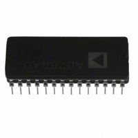
AD760AQ Analog Devices Inc, AD760AQ Datasheet - Page 10

AD760AQ
Manufacturer Part Number
AD760AQ
Description
Digital-Analog Converter IC
Manufacturer
Analog Devices Inc
Series
DACPORT®r
Datasheet
1.AD760AQ.pdf
(12 pages)
Specifications of AD760AQ
Rohs Status
RoHS non-compliant
Settling Time
6µs
Number Of Bits
16
Data Interface
Serial, Parallel
Number Of Converters
1
Voltage Supply Source
Dual ±
Power Dissipation (max)
725mW
Operating Temperature
-40°C ~ 85°C
Mounting Type
Through Hole
Package / Case
28-CDIP (0.600", 15.24mm)
Lead Free Status / RoHS Status
Available stocks
Company
Part Number
Manufacturer
Quantity
Price
Company:
Part Number:
AD760AQZ
Manufacturer:
INTEL
Quantity:
32
AD760
Byte Mode Operation is enabled by setting SER high, which
configures DB0–DB7 as data inputs. In this mode HBE and
LBE are used to identify the data as either the high byte or the
low byte of the 16-bit word. The user can load the data in either
order into the first rank latch using the rising edge of the CS
signal as shown in Figure 1a. The status of Pin 17 when CLR is
strobed determines whether the AD760 clears to unipolar or
bipolar zero. (But it cannot be hardwired to the desired state, as
in the serial mode.)
NOTE: CS is edge triggered. HBE, LBE, CLR, SER, CAL, and
LDAC are level triggered.
USING THE OUTPUT MULTIPLEXER
The onboard multiplexer allows the user to isolate the load from
the voltage variations at V
the glitch-impulse at MUX
should be tied to a voltage equal to the DAC’s negative
full-scale voltage. Since the DAC is loaded with the contents of
its first-rank latch before completing calibration, the DAC
should be programmed to negative full scale before calibrating.
This will minimize the voltage excursions of MUX
beginning and end of calibration. If the glitch-impulse at the
beginning of calibration is not important, yet the user wants to
minimize the recovery time at MUX
to the voltage that corresponds to the data in the first-rank latch
before calibration is initiated.
The multiplexer series on-resistance limits its load-drive capability.
To attain 16-bit linearity, MUX
suitable op amp. The amplifier open loop-gain and common-
mode rejection contribute to gain error whereas the linearity of
these parameters affect the relative accuracy (or integral nonlin-
earity). In general, the amplifier linearity is not specified so its
effects must be determined empirically. Using the AD707, as
shown in Figure 9, the overall linearity error is within 0.5 LSB.
The AD707C/T initial voltage offset and its temperature coeffi-
cient will not contribute more than 0.1 LSB to the Bipolar Zero
Error over the entire operating temperature range. The settling
time to 1/2 LSB is typically 100 µs for a 20 V step. For applica-
tions that require faster settling, the AD820 can be used to
attain full-scale settling to within a 1/2 LSB in 20 µs. The addi-
tional linearity error from the AD820 will be no more than
0.25 LSB.
OUT
OUT
AD760
during calibration. To minimize
–V
, the multiplexer input, MUX
+V
OUT
EE
3
4
CC
OUT
must be buffered with a
24
23
27
28
22
1
Figure 10. Using the AD760 with an External MUX
, MUX
AGND
V
MUX
MUX
SPAN/
BIP OFF
CALOK
OUT
OUT
IN
IN
should be set
OUT
at the
6
8
2
IN
,
ADG419
–10–
–V
+V
4
EE
7
CC
USING AN EXTERNAL MULTIPLEXER
An external multiplexer like the ADG419 allows the user to
minimize the glitch impulse when holding the output to any
predetermined voltage during calibration. The ADG419 can be
used with a high speed op amp like the AD829, as shown in Fig-
ure 10, to attain the fastest possible settling time while main-
taining 16-bit linearity. The settling time to 1/2 LSB for a 20 V
step is typically 10 µs.
AD760 TO MC68HC11 (SPI* BUS) INTERFACE
The AD760 interface to the Motorola SPI (serial peripheral in-
terface) is shown in Figure 11. The MOSI, SCK, and SS pins of
the HC11 are respectively connected to the S
pins of the AD760. The majority of the interfacing issues are
taken care of in the software initialization. A typical routine such
as the one shown below begins by initializing the state of the
various SPI data and control registers.
The most significant data byte (MSBY) is then retrieved from
memory and processed by the SENDAT subroutine. The SS
pin is driven low by indexing into the PORTD data register and
clearing Bit 5. The MSBY is then sent to the SPI data
register where it is automatically transferred to the AD760.
*SPI is a registered trademark of Motorola.
1
Figure 9. Buffering the AD760 Internal MUX
AD760
1nF
–V
+V
EE
3
4
CC
23
24
27
28
22
1
2
3
0.1µF
MUX
SPAN/
BIP OFF
V
MUX
AGND
CALOK
AD829
OUT
–V
+V
O UT
I N
4
7
EE
CC
0.1µF
5
6
100pF
60pF
3
2
AD707
AD820
OR
+V
–V
4
7
CC
EE
0.1µF
0.1µF
1k
IN
6
OUT
1k
, CS and LDAC
OUTPUT
REV. A


