AD7528AQ Analog Devices Inc, AD7528AQ Datasheet
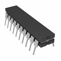
Digital-Analog Converter IC

AD7528AQ

Manufacturer Part Number
AD7528AQ
Description
Digital-Analog Converter IC
Manufacturer
Analog Devices Inc
Datasheet

Specifications of AD7528AQ

Rohs Status
RoHS non-compliant
Settling Time
400ns
Number Of Bits
8
Number Of Converters
2
Voltage Supply Source
Single Supply
Power Dissipation (max)
450mW
Operating Temperature
-40°C ~ 85°C
Mounting Type
Through Hole
Package / Case
20-CDIP (0.300", 7.62mm)
Data Interface
-
Lead Free Status / RoHS Status

Available stocks

Company
Part Number
Manufacturer
Quantity
Price
Part Number:
AD7528AQ
Manufacturer:
a
Quantity:
75
Part Number:
AD7528AQ
Manufacturer:
ADI
Quantity:
940
a
GENERAL DESCRIPTION
The AD7528 is a monolithic dual 8-bit digital/analog converter
featuring excellent DAC-to-DAC matching. It is available in
skinny 0.3" wide 20-lead DIPs and in 20-lead surface mount
packages.
Separate on-chip latches are provided for each DAC to allow
easy microprocessor interface.
Data is transferred into either of the two DAC data latches via a
common 8-bit TTL/CMOS compatible input port. Control
input DAC A/DAC B determines which DAC is to be loaded.
The AD7528’s load cycle is similar to the write cycle of a ran-
dom access memory and the device is bus compatible with most
8-bit microprocessors, including 6800, 8080, 8085, Z80.
The device operates from a +5 V to +15 V power supply, dis-
sipating only 20 mW of power.
Both DACs offer excellent four quadrant multiplication charac-
teristics with a separate reference input and feedback resistor for
each DAC.
PRODUCT HIGHLIGHTS
1. DAC-to-DAC matching: since both of the AD7528 DACs are
2. Small package size: combining the inputs to the on-chip DAC
REV. B
Information furnished by Analog Devices is believed to be accurate and
reliable. However, no responsibility is assumed by Analog Devices for its
use, nor for any infringements of patents or other rights of third parties
which may result from its use. No license is granted by implication or
otherwise under any patent or patent rights of Analog Devices.
fabricated at the same time on the same chip, precise match-
ing and tracking between DAC A and DAC B is inherent.
The AD7528’s matched CMOS DACs make a whole new
range of applications circuits possible, particularly in the
audio, graphics and process control areas.
latches into a common data bus and adding a DAC A/DAC B
select line has allowed the AD7528 to be packaged in either a
small 20-lead DIP, SOIC or PLCC.
FEATURES
On-Chip Latches for Both DACs
+5 V to +15 V Operation
DACs Matched to 1%
Four Quadrant Multiplication
TTL/CMOS Compatible
Latch Free (Protection Schottkys not Required)
APPLICATIONS
Digital Control of:
Gain/Attenuation
Filter Parameters
Stereo Audio Circuits
X-Y Graphics
One Technology Way, P.O. Box 9106, Norwood, MA 02062-9106, U.S.A.
Tel: 781/329-4700
Fax: 781/326-8703
Model
AD7528JN
AD7528KN –40 C to +85 C
AD7528LN –40 C to +85 C
AD7528JP
AD7528KP
AD7528LP
AD7528JR
AD7528KR –40 C to +85 C
AD7528LR
AD7528AQ –40 C to +85 C
AD7528BQ –40 C to +85 C
AD7528CQ –40 C to +85 C
AD7528SQ
AD7528TQ –55 C to +125 C
AD7528UQ –55 C to +125 C
NOTES
1
2
3
INPUTS
Analog Devices reserves the right to ship side-brazed ceramic in lieu of cerdip. Parts
Processing to MIL-STD-883C, Class B is available. To order, add suffix “/883B” to
N = Plastic DIP; P = Plastic Leaded Chip Carrier; Q = Cerdip; R = SOIC.
DAC A/
will be marked with cerdip designator “Q.”
part number. For further information, see Analog Devices’ 1990 Military Products
Databook.
DAC B
DGND
DATA
V
WR
CS
DD
DB7
DB0
2
FUNCTIONAL BLOCK DIAGRAM
Buffered Multiplying DAC
Temperature
Ranges
–40 C to +85 C
–40 C to +85 C
–40 C to +85 C
–40 C to +85 C
–40 C to +85 C
–40 C to +85 C
–55 C to +125 C
CONTROL
BUFFER
LOGIC
INPUT
World Wide Web Site: http://www.analog.com
ORDERING GUIDE
LATCH
LATCH
CMOS Dual 8-Bit
Relative
Accuracy Error
1 LSB
1/2 LSB
1/2 LSB
1 LSB
1/2 LSB
1/2 LSB
1 LSB
1/2 LSB
1/2 LSB
1 LSB
1/2 LSB
1/2 LSB
1 LSB
1/2 LSB
1/2 LSB
AD7528
© Analog Devices, Inc., 1998
V
V
REF
REF
DAC B
DAC A
A
B
1
AD7528
Gain
4 LSB N-20
2 LSB N-20
1 LSB N-20
4 LSB P-20A
2 LSB P-20A
1 LSB P-20A
4 LSB R-20
2 LSB R-20
1 LSB R-20
4 LSB Q-20
2 LSB Q-20
1 LSB Q-20
4 LSB Q-20
2 LSB Q-20
1 LSB Q-20
Package
Options
R
AGND
R
OUT A
OUT B
FB
FB
A
B
3

Related parts for AD7528AQ

AD7528AQ Summary of contents

Page 1

... AD7528LP – +85 C 1/2 LSB AD7528JR – + LSB AD7528KR – +85 C 1/2 LSB AD7528LR – +85 C 1/2 LSB AD7528AQ – + LSB AD7528BQ – +85 C 1/2 LSB AD7528CQ – +85 C 1/2 LSB AD7528SQ – +125 C 1 LSB AD7528TQ – +125 C 1/2 LSB AD7528UQ – ...

Page 2

AD7528–SPECIFICATIONS Parameter Version 2 STATIC PERFORMANCE Resolution All Relative Accuracy Differential Nonlinearity All Gain Error Gain Temperature Coefficient Gain/ Temperature All ...

Page 3

Parameter Version CHANNEL-TO-CHANNEL ISOLATION OUT B All REF OUT A REF DIGITAL CROSSTALK All HARMONIC DISTORTlON All NOTES 1 Temperature Ranges are Versions: – + ...

Page 4

AD7528 INTERFACE LOGIC INFORMATION DAC Selection: Both DAC latches share a common 8-bit input port. The con- trol input DAC A/DAC B selects which DAC can accept data from the input port. Mode Selection: Inputs CS and WR control the ...

Page 5

V DD DB0 DATA INPUT LATCH INPUTS BUFFER DB7 AD7528 DAC A/ DAC B CONTROL CS LOGIC WR LATCH DGND NOTES: 1 R1, R2 AND R3, R4 USED ONLY IF GAIN ADJUSTMENT IS REQUIRED. SEE TABLE III FOR RECOMMENDED VALUES. ...

Page 6

AD7528 APPLICATIONS INFORMATION Application Hints To ensure system performance consistent with AD7528 specifi- cations, careful attention must be given to the following points: 1. GENERAL GROUND MANAGEMENT transient voltages between the AD7528 AGND and DGND can cause noise ...

Page 7

MICROPROCESSOR INTERFACE A0–A15 ADDRESS BUS A** ADDRESS V DECODE MA LOGIC CPU A + 1** 6800 2 D0–D7 DATA BUS *ANALOG CIRCUITRY HAS BEEN OMITTED FOR CLARITY **A = DECODED 7528 ADDR DAC DECODED 7528 ...

Page 8

AD7528 DIGITALLY CONTROLLED DUAL TELEPHONE ATTENUATOR In this configuration the AD7528 functions as a 2-channel digi- tally controlled attenuator. Ideal for stereo audio and telephone signal level control applications. Table IV gives input codes vs. attenuation for ...

Related keywords