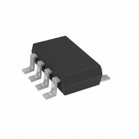
AD7273BUJZ-REEL7 Analog Devices Inc, AD7273BUJZ-REEL7 Datasheet - Page 7

AD7273BUJZ-REEL7
Manufacturer Part Number
AD7273BUJZ-REEL7
Description
10-Bit 3MSPS SAR ADC I.C.
Manufacturer
Analog Devices Inc
Datasheet
1.AD7273BUJZ-REEL7.pdf
(28 pages)
Specifications of AD7273BUJZ-REEL7
Number Of Bits
10
Sampling Rate (per Second)
3M
Data Interface
DSP, MICROWIRE™, QSPI™, Serial, SPI™
Number Of Converters
1
Power Dissipation (max)
18mW
Voltage Supply Source
Single Supply
Operating Temperature
-40°C ~ 125°C
Mounting Type
Surface Mount
Package / Case
SOT-23-8 Thin, TSOT-23-8
Lead Free Status / RoHS Status
Lead free / RoHS Compliant
TIMING SPECIFICATIONS
V
are specified with tr = tf = 2 ns (10% to 90% of V
Table 4.
Parameter
f
t
t
t
t
t
t
t
t
t
t
t
t
1
2
3
4
5
SCLK
CONVERT
QUIET
1
2
3
4
5
6
7
8
9
POWER-UP
Sample tested during initial release to ensure compliance. All timing specifications given are with a 10 pF load capacitance. With a load capacitance greater than this
value, a digital buffer or latch must be used.
Mark/space ratio for the SCLK input is 40/60 to 60/40.
Minimum f
The time required for the output to cross the V
See the Power-Up Times section
4
4
4
DD
2
SDATA
SDATA
= 2.35 V to 3.6 V; V
SCLK
SCLK
5
SCLK
V
V
IH
IL
at which specifications are guaranteed.
Figure 2. Access Time After SCLK Falling Edge
Limit at T
AD7273/AD7274
500
48
14 × t
12 × t
4
3
6
4
15
0.4 t
0.4 t
5
14
5
4.2
1
Figure 3. Hold Time After SCLK Falling Edge
SCLK
SCLK
SCLK
SCLK
REF
MIN
t
7
t
4
= 2.35 to V
, T
MAX
DD
IH
; T
or V
A
IL
= T
voltage.
MIN
DD
kHz min
MHz max
ns min
ns min
ns min
ns max
ns max
ns max
ns max
μs max
Unit
ns min
ns min
ns min
ns min
) and timed from a voltage level of 1.6 V.
to T
MAX
V
V
3
IH
IL
, unless otherwise noted.
Rev. 0 | Page 7 of 28
Description
AD7274
AD7273
Minimum quiet time required between bus relinquish and start of
next conversion
Minimum CS pulse width
CS to SCLK setup time
Delay from CS until SDATA three-state disabled
Data access time after SCLK falling edge
SCLK low pulse width
SCLK high pulse width
SCLK to data valid hold time
SCLK falling edge to SDATA three-state
SCLK falling edge to SDATA three-state
CS rising edge to SDATA three-state
Power-up time from full power-down
SDATA
SCLK
1
Guaranteed by characterization. All input signals
Figure 4. SCLK Falling Edge SDATA Three-State
t
8
AD7273/AD7274
1.4V


