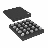
AD7147A-1ACBZ-RL Analog Devices Inc, AD7147A-1ACBZ-RL Datasheet - Page 31

AD7147A-1ACBZ-RL
Manufacturer Part Number
AD7147A-1ACBZ-RL
Description
CAPACITANCE TO DIGITAL CONVERTER
Manufacturer
Analog Devices Inc
Series
CapTouch™r
Type
Capacitive Sensor Controllerr
Datasheet
1.AD7147AACBZ-RL.pdf
(68 pages)
Specifications of AD7147A-1ACBZ-RL
Resolution (bits)
16 b
Data Interface
I²C, Serial
Voltage Supply Source
Single Supply
Voltage - Supply
2.6 V ~ 3.6 V
Operating Temperature
-40°C ~ 85°C
Mounting Type
Surface Mount
Package / Case
25-WLCSP
Lead Free Status / RoHS Status
Lead free / RoHS Compliant
Sampling Rate (per Second)
-
Lead Free Status / RoHS Status
Lead free / RoHS Compliant
OUTPUTS
AC
The AD7147A measures the capacitance between CINx and
ground. Any capacitance to ground on the signal path between
the CINx pins and the sensor is included in the AD7147A
conversion result.
To eliminate stray capacitance to ground, the AC
be used to shield the connection between the sensor and CINx,
as shown in Figure 46. The plane around the sensors should also
be connected to AC
The AC
signal on CINx. Therefore, there is no ac current between CINx
and AC
affect the CINx charge transfer.
Using AC
means that the AD7147A can be placed up to 10 cm away from
the sensors. This allows the AD7147A to be placed on a separate
PCB from that of the sensors if the connections between the
sensors and the CINx inputs are correctly shielded using
AC
GENERAL-PURPOSE INPUT/OUTPUT (GPIO)
The AD7147A has one GPIO pin. It can be configured as an input
or an output. The GPIO_SETUP Bits[13:12] in the STAGE_LOW_
INT_ENABLE register determine how the GPIO pin is configured.
Table 17. GPIO_SETUP Bits
GPIO_SETUP
00
01
10
11
SHIELD
SHIELD
SHIELD
SHIELD
.
OUTPUT
SHIELD
, and any capacitance between these pins does not
output is the same signal waveform as the excitation
eliminates capacitance-to-ground pickup, which
SHIELD
.
Figure 46. AC
GPIO Configuration
GPIO disabled
Input
Output low
Output high
SHIELD
CIN0
CIN1
CIN2
CIN3
SHIELD
AC
AD7147A
SHIELD
signal should
GND
Rev. B | Page 31 of 68
When the GPIO is configured as an output, the voltage level on
the pin is set to either a low level or a high level, as defined by
the GPIO_SETUP bits (see Table 17).
The GPIO_INPUT_CONFIG bits in the STAGE_LOW_INT_
ENABLE register determine the response of the AD7147A to a
signal on the GPIO pin when the GPIO is configured as an
input. The GPIO can be configured as either active high or
active low, as well as either edge triggered or level triggered (see
Table 18).
Table 18. GPIO_INPUT_CONFIG Bits
GPIO_INPUT_CONFIG
00
01
10
11
When GPIO is configured as an input, it triggers the interrupt
output on the AD7147A.
Table 16 lists the interrupt output behavior for each of the GPIO
configuration setups.
USING THE GPIO TO TURN ON/OFF AN LED
The GPIO on the AD7147A can be used to turn an LED on and
off by setting the GPIO as either output high or low. Setting the
GPIO output high turns on the LED; setting the GPIO output
low turns off the LED. The GPIO pin connects to a transistor
that provides the drive current for the LED. Suitable transistors
include the KTC3875 from Korea Electronics Co., Ltd. (KEC).
Figure 47. Controlling an LED Using the GPIO
AD7147A
GPIO
GPIO Configuration
Triggered on negative level (active low)
Triggered on positive edge (active high)
Triggered on negative edge (active low)
Triggered on positive level (active high)
OR SIMILAR
KTC3875
V
CC
AD7147A


