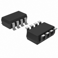
AD5662BRJZ-1REEL7 Analog Devices Inc, AD5662BRJZ-1REEL7 Datasheet - Page 9

AD5662BRJZ-1REEL7
Manufacturer Part Number
AD5662BRJZ-1REEL7
Description
IC,D/A CONVERTER,SINGLE,16-BIT,CMOS,TSSOP,8PIN
Manufacturer
Analog Devices Inc
Series
nanoDAC™r
Datasheet
1.AD5662BRJZ-2REEL7.pdf
(24 pages)
Specifications of AD5662BRJZ-1REEL7
Design Resources
4 mA to 20 mA Process Control Loop Using AD5662 (CN0009) 16-Bit Fully Isolated Voltage Output Module Using AD5662, ADuM1401, and External Amplifiers (CN0063) 16-Bit Fully Isolated 4 mA to 20 mA Output Module Using AD5662, ADuM1401, and External Amplifiers (CN0064)
Settling Time
8µs
Number Of Bits
16
Data Interface
DSP, MICROWIRE™, QSPI™, Serial, SPI™
Number Of Converters
1
Voltage Supply Source
Single Supply
Power Dissipation (max)
750µW
Operating Temperature
-40°C ~ 125°C
Mounting Type
Surface Mount
Package / Case
SOT-23-8
Lead Free Status / RoHS Status
Lead free / RoHS Compliant
Other names
AD5662BRJZ-1REEL7TR
Available stocks
Company
Part Number
Manufacturer
Quantity
Price
Company:
Part Number:
AD5662BRJZ-1REEL7
Manufacturer:
MITSUBISHI
Quantity:
120
–0.22
–0.04
–0.06
–0.08
–0.01
–0.12
–0.14
–0.16
–0.18
–0.20
–0.5
–1.0
–1.5
–2.0
–2.5
–0.5
–1.0
–1.5
–2.0
1.5
1.0
0.5
1.0
0.5
Figure 10. Gain Error and Full-Scale Error vs. Temperature
0
0
0
–40
–40
Figure 11. Zero-Scale and Offset Error vs. Temperature
2.7
Figure 12. Gain Error and Full-Scale Error vs. Supply
V
DD
OFFSET ERROR
–20
–20
= 5V
GAIN ERROR
FULL-SCALE ERROR
ZERO-SCALE ERROR
3.2
FULL-SCALE ERROR
0
0
GAIN ERROR
3.7
TEMPERATURE ( ° C)
TEMPERATURE ( ° C)
20
20
V
40
40
DD
4.2
(V)
60
60
4.7
80
80
100
100
5.2
120
120
Rev. A | Page 9 of 24
–0.05
–0.10
–0.15
–0.20
–0.25
–0.5
–1.0
–1.5
–2.0
–2.5
0.20
0.15
0.10
0.05
1.0
0.5
20
18
16
14
12
10
Figure 15. Headroom at Rails vs. Source and Sink Current
0
8
6
4
2
0
0
2.7
–5
Figure 13. Zero-Scale and Offset Error vs. Supply
T
V
T
V
T
A
A
A
DD
DD
–4
= 25 ° C
= 25 ° C
= 25 ° C
Figure 14. I
= V
= V
3.2
REF
REF
–3
DAC LOADED WITH
FULL SCALE –
SOURCING CURRENT
= 5V, 3V
= 5.5V
–2
DD
Histogram with V
3.7
–1
I
V
DD
I (mA)
DD
0
( μ A)
4.2
(V)
DAC LOADED WITH
ZERO SCALE –
SINKING CURRENT
ZERO-SCALE ERROR
1
DD
OFFSET ERROR
= 5.5 V
2
4.7
3
5.2
4
AD5662
5


