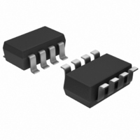
AD5620BRJ-1REEL7 Analog Devices Inc, AD5620BRJ-1REEL7 Datasheet - Page 6

AD5620BRJ-1REEL7
Manufacturer Part Number
AD5620BRJ-1REEL7
Description
IC,D/A CONVERTER,SINGLE,12-BIT,CMOS,TSSOP,8PIN
Manufacturer
Analog Devices Inc
Series
nanoDAC™r
Datasheet
1.AD5620ARJZ-1500RL7.pdf
(28 pages)
Specifications of AD5620BRJ-1REEL7
Design Resources
Single-Ended-to-Differential Converters for Voltage Output and Current Output DACs Using AD8042 (CN0143) Amplitude Control Circuit for AD9834 Waveform Generator (CN0156)
Settling Time
8µs
Number Of Bits
12
Data Interface
DSP, MICROWIRE™, QSPI™, Serial, SPI™
Number Of Converters
1
Voltage Supply Source
Single Supply
Power Dissipation (max)
2.5mW
Operating Temperature
-40°C ~ 105°C
Mounting Type
Surface Mount
Package / Case
SOT-23-8
Lead Free Status / RoHS Status
Contains lead / RoHS non-compliant
AD5620/AD5640/AD5660
Parameter
LOGIC INPUTS
POWER REQUIREMENTS
1
2
3
4
Part is functional with V
Temperature range is −40°C to +105°C, typical at +25°C.
Linearity calculated using a reduced code range: AD5660 (Code 511 to Code 65024); AD5640 (Code 128 to Code 16256); AD5620 (Code 32 to Code 4064). Output
unloaded.
Guaranteed by design and characterization; not production tested.
Input Current
V
V
Pin Capacitance
V
I
I
DD
DD
INL
INH
DD
V
V
V
V
(Normal Mode)
(All Power-Down Modes)
, Input Low Voltage
, Input High Voltage
DD
DD
DD
DD
= 2.7 V to 3.3 V
= 2.7 V to 3.3 V
= 2.7 V to 3.3 V
= 2.7 V to 3.3 V
4
DD
up to 5.5 V.
A Grade
±1
0.8
2
3
2.7
3.3
0.55
0.65
0.2
0.25
2
B Grade
±1
0.8
2
3
2.7
3.3
0.55
0.65
0.2
0.25
2
Rev. F | Page 6 of 28
C Grade
±1
0.8
2
2.7
3.3
3
0.55
0.65
0.2
0.25
2
V max
Unit
μA max
V min
pF max
V min
V max
mA typ
mA max
μA typ
μA max
Conditions/Comments
All digital inputs
V
V
All digital inputs at 0 V or V
DAC active and excluding load current
V
V
V
V
DD
DD
IH
IH
IH
IH
= V
= V
= V
= V
= 3 V
= 3 V
DD
DD
DD
DD
and V
and V
and V
and V
IL
IL
IL
IL
= GND
= GND
= GND
= GND
DD


