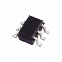
AD5612BKSZ-2REEL7 Analog Devices Inc, AD5612BKSZ-2REEL7 Datasheet - Page 21

AD5612BKSZ-2REEL7
Manufacturer Part Number
AD5612BKSZ-2REEL7
Description
IC,D/A CONVERTER,SINGLE,10-BIT,CMOS,TSSOP,6PIN
Manufacturer
Analog Devices Inc
Series
nanoDAC™r
Datasheet
1.AD5622AKSZ-2REEL7.pdf
(24 pages)
Specifications of AD5612BKSZ-2REEL7
Settling Time
6µs
Number Of Bits
10
Data Interface
I²C, Serial
Number Of Converters
1
Voltage Supply Source
Single Supply
Power Dissipation (max)
500µW
Operating Temperature
-40°C ~ 85°C
Mounting Type
Surface Mount
Package / Case
SC-70-6, SC-88, SOT-363
Lead Free Status / RoHS Status
Lead free / RoHS Compliant
Available stocks
Company
Part Number
Manufacturer
Quantity
Price
Part Number:
AD5612BKSZ-2REEL7
Manufacturer:
ADI/亚德诺
Quantity:
20 000
APPLICATIONS
CHOOSING A REFERENCE AS POWER SUPPLY
The AD5602/AD5612/AD5622 come in tiny SC70 packages
with less than 100 μA supply current, thereby making the
choice of reference dependent upon the application
requirement. For space-saving applications, the ADR425 is
available in an SC70 package with excellent drift at 3ppm/°C. It
also provides very good noise performance at 3.4 μV p-p in the
0.1 Hz to 10 Hz range.
Because the supply current required by the AD5602/AD5612/
AD5622 DACs is extremely low, they are ideal for low supply
applications. The ADR293 voltage reference is recommended in
this case. This requires 15 μA of quiescent current and can
therefore drive multiple DACs in the one system, if required.
Examples of some recommended precision references for use as
supplies to the AD5602/AD5612/AD5622 are shown in Table 8.
Table 8. Recommended Precision References
Part
No.
ADR435
ADR425
ADR02
ADR395
BIPOLAR OPERATION
The AD5602/AD5612/AD5622 have been designed for single-
supply operation, but a bipolar output range is also possible
using the circuit in Figure 50. The circuit in Figure 50 gives an
output voltage range of ±5 V. Rail-to-rail operation at the
amplifier output is achievable using an AD820 or an OP295 as
the output amplifier.
The output voltage for any input code can be calculated as
where:
D represents the input code in decimal.
n represents the bit resolution of the DAC.
V
O
7V
=
SDA
SCL
⎡
⎢
⎣
Initial
Accuracy
(mV max)
±6
±6
±5
±6
ADR425
V
DD
×
Figure 49. ADR425 as Power Supply
⎛
⎜
⎝
2
D
n
⎞
⎟
⎠
×
Temperature
Drift
(ppm/°C max)
3
3
3
25
⎛
⎜
⎝
5V
R1
AD5602/
AD5612/
AD5622
R1
+
R2
⎞
⎟
⎠
−
V
DD
V
0.1 Hz to 10 Hz Noise
(μV p-p typ)
3.4
3.4
15
5
OUT
×
⎛
⎜
⎝
= 0V TO 5V
R2
R1
⎞
⎟
⎠
⎤
⎥
⎦
Rev. B | Page 21 of 24
With V
This is an output voltage range of ±5 V with 0x000 corresponding
to a −5 V output, and 0xFFF corresponding to a +5 V output.
POWER SUPPLY BYPASSING AND GROUNDING
When accuracy is important in a circuit, it is helpful to carefully
consider the power supply and ground return layout on the
board. The printed circuit board containing the AD5602/
AD5612/AD5622 should have separate analog and digital
sections, each having its own area of the board. If the AD5602,
AD5612, or AD5622 is in a system where other devices require
an AGND to DGND connection, the connection should be
made at one point only. This ground point should be as close as
possible to the AD5602/AD5612/AD5622.
The power supply to the AD5602/AD5612/AD5622 should be
bypassed with 10 μF and 0.1 μF capacitors. The capacitors
should be physically as close as possible to the device with the
0.1 μF capacitor ideally right up against the device. The 10 μF
capacitors are the tantalum bead type. It is important that the
0.1 μF capacitor has low effective series resistance (ESR) and
effective series inductance (ESI), such as common ceramic
types. This 0.1 μF capacitor provides a low impedance path to
ground for high frequencies caused by transient currents due to
internal logic switching.
The power supply line should have as large a trace as possible to
provide a low impedance path and reduce glitch effects on the
supply line. Clocks and other fast switching digital signals
should be shielded from other parts of the board by digital
ground. Avoid crossover of digital and analog signals if possible.
When traces cross on opposite sides of the board, ensure that
they run at right angles to each other to reduce feedthrough
effects through the board. The best board layout technique is
the microstrip technique where the component side of the
board is dedicated to the ground plane only and the signal
traces are placed on the solder side. However, the microstrip
technique is not always possible with a 2-layer board.
+5V
V
Figure 50. Bipolar Operation with the AD5602/AD5612/AD5622
O
DD
10µF
=
= 5 V, R1 = R2 = 10 kΩ
⎛
⎜
⎝
10
2
×
n
0.1µF
D
⎞
⎟
⎠
−
V
5
DD
SDA SCL
V
AD5602/AD5612/AD5622
AD5602/
AD5612/
AD5622
10kΩ
R1
V
OUT
AD820/
OP295
+5V
–5V
10kΩ
R2
±5V OUT


