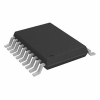
AD5445YRU-REEL7 Analog Devices Inc, AD5445YRU-REEL7 Datasheet - Page 22

AD5445YRU-REEL7
Manufacturer Part Number
AD5445YRU-REEL7
Description
IC,D/A CONVERTER,SINGLE,12-BIT,CMOS,TSSOP,20PIN
Manufacturer
Analog Devices Inc
Datasheet
1.AD5445YRUZ.pdf
(32 pages)
Specifications of AD5445YRU-REEL7
Rohs Status
RoHS non-compliant
Settling Time
80ns
Number Of Bits
12
Data Interface
Parallel
Number Of Converters
1
Voltage Supply Source
Single Supply
Power Dissipation (max)
25µW
Operating Temperature
-40°C ~ 125°C
Mounting Type
Surface Mount
Package / Case
20-TSSOP
For Use With
EVAL-AD5445EBZ - BOARD EVALUATION FOR AD5445
Lead Free Status / RoHS Status
AD5424/AD5433/AD5445
Provided the DAC switches are driven from true wideband low
impedance sources (V
quently, the slew rate and settling time of a voltage switching
DAC circuit is determined largely by the output op amp. To
obtain minimum settling time in this configuration, it is impor-
tant to minimize capacitance at the V
node in this application) of the DAC. This is done by using low
inputs capacitance buffer amplifiers and careful board design.
Most single-supply circuits include ground as part of the analog
signal range, which in turns requires an amplifier that can
handle rail-to-rail signals. There is a large range of single-supply
amplifiers available from Analog Devices.
PARALLEL INTERFACE
Data is loaded to the AD5424/AD5433/AD5445 in the format
of an 8-, 10-, or 12-bit parallel word. Control lines CS and R/ W
allow data to be written to or read from the DAC register. A
write event takes place when CS and R/ W are brought low, data
available on the data lines fills the shift register, and the rising
edge of CS latches the data and transfers the latched data-word
to the DAC register. The DAC latches are not transparent, thus
a write sequence must consist of a falling and rising edge on CS
to ensure that data is loaded to the DAC register and its analog
equivalent is reflected on the DAC output.
A read event takes place when R/ W is held high and CS is
brought low. New data is loaded from the DAC register back to
the input register and out onto the data line where it can be read
back to the controller for verification or diagnostic purposes.
MICROPROCESSOR INTERFACING
ADSP-21xx-to-AD5424/AD5433/AD5445 Interface
Figure 56 shows the AD5424/AD5433/AD5445 interfaced to
the ADSP-21xx series of DSPs as a memory-mapped device. A
single wait state may be necessary to interface the AD5424/
AD5433/AD5445 to the ADSP-21xx, depending on the clock
speed of the DSP. The wait state can be programmed via the
data memory wait state control register of the ADSP-21xx (see
the ADSP-21xx family user’s manual for details).
ADSP-21xx*
*ADDITIONAL PINS OMITTED FOR CLARITY
DATA 0 TO
ADDR
DATA 23
ADRR
Figure 56. ADSP21xx-to-AD5424/AD5433/AD5445 Interface
0
DMS
TO
WR
13
DECODER
ADDRESS
IN
and AGND), they settle quickly. Conse-
ADDRESS BUS
DATA BUS
REF
node (voltage output
R/W
DB0 TO DB11
CS
AD5424/
AD5433/
AD5445*
Rev. B | Page 22 of 32
8xC51-to-AD5424/AD5433/AD5445 Interface
Figure 57 shows the interface between the AD5424/AD5433/
AD5445 and the 8xC51 family of DSPs. To facilitate external
data memory access, the address latch enable (ALE) mode is
enabled. The low byte of the address is latched with this output
pulse during access to external memory. AD0 to AD7 are the
multiplexed low order addresses and data bus and require
strong internal pull-ups when emitting 1s. During access to
external memory, A8 to A15 are the high order address bytes.
Since these ports are open drained, they also require strong
internal pull-ups when emitting 1s.
ADSP-BF5xx-to-AD5424/AD5433/AD5445 Interface
Figure 58 shows a typical interface between the AD5424/
AD5433/AD5445 and the ADSP-BF5xx family of DSPs. The
asynchronous memory write cycle of the processor drives the
digital inputs of the DAC. The AMS x line is actually four
memory select lines. Internal ADDR lines are decoded into
AMS
the interface is a standard handshaking operation.
8051*
ADSP-BF5xx
*ADDITIONAL PINS OMITTED FOR CLARITY
*ADDITIONAL PINS OMITTED FOR CLARITY
AD0 TO AD7
A8 TO A15
DATA 0 TO
ADDR
3-0
DATA 23
ADRR
Figure 58. ADSP-BF5xx-to-AD5424/AD5433/AD5445 Interface
, these lines are then inserted as chip selects. The rest of
AMSx
1
AWE
Figure 57. 8xC51-to-AD5424/AD5433/AD5445 Interface
ALE
TO
WR
19
ADDRESS
DECODER
ADDRESS
DECODER
LATCH
8-BIT
ADDRESS BUS
DATA BUS
ADDRESS BUS
DATA BUS
R/W
DB0 TO DB11
R/W
DB0 TO DB11
CS
CS
AD5424/
AD5433/
AD5445*
AD5424/
AD5433/
AD5445*


