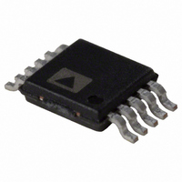
AD5444YRM Analog Devices Inc, AD5444YRM Datasheet - Page 6

AD5444YRM
Manufacturer Part Number
AD5444YRM
Description
IC,D/A CONVERTER,SINGLE,12-BIT,CMOS,TSSOP,10PIN
Manufacturer
Analog Devices Inc
Datasheet
1.AD5446YRMZ.pdf
(28 pages)
Specifications of AD5444YRM
Settling Time
16ns
Number Of Bits
12
Data Interface
Serial
Number Of Converters
1
Voltage Supply Source
Single Supply
Power Dissipation (max)
50.5µW
Operating Temperature
-40°C ~ 125°C
Mounting Type
Surface Mount
Package / Case
10-MSOP, Micro10™, 10-uMAX, 10-uSOP
Lead Free Status / RoHS Status
Contains lead / RoHS non-compliant
Available stocks
Company
Part Number
Manufacturer
Quantity
Price
Part Number:
AD5444YRMZ
Manufacturer:
ADI/亚德诺
Quantity:
20 000
Part Number:
AD5444YRMZ-REEL7
Manufacturer:
ADI/亚德诺
Quantity:
20 000
AD5444/AD5446
ABSOLUTE MAXIMUM RATINGS
T
100 mA do not cause SCR latch-up.
Table 3.
Parameter
V
V
I
Logic Inputs and Outputs
Input Current (All Pins Except Supplies)
Operating Temperature Range
Extended (Y Version)
Storage Temperature Range
Junction Temperature
10-lead MSOP θ
Lead Temperature, Soldering (10 sec)
IR Reflow, Peak Temperature (<20 sec)
1
OUT
Overvoltages at SCLK, SYNC , and SDIN are clamped by internal diodes.
DD
REF
A
= 25°C, unless otherwise noted. Transient currents of up to
1, I
, R
to GND
FB
OUT
to GND
2 to GND
JA
Thermal Impedance
1
Rating
−0.3 V to +7 V
−12 V to +12 V
−0.3 V to +7 V
−0.3 V to V
±10 mA
−40°C to +125°C
−65°C to +150°C
150°C
206°C/W
300°C
235°C
DD
+ 0.3 V
Rev. C | Page 6 of 28
Stresses above those listed under Absolute Maximum Ratings
may cause permanent damage to the device. This is a stress
rating only; functional operation of the device at these or any
other conditions above those indicated in the operational
section of this specification is not implied. Exposure to absolute
maximum rating conditions for extended periods may affect
device reliability.
Only one absolute maximum rating can be applied at any one
time.
ESD CAUTION
OUTPUT
Figure 4. Load Circuit for SDO Timing Specifications
PIN
TO
C
20pF
L
200µA
200µA
I
I
OL
OH
V
OH (MIN)
2
+V
OL (MAX)


