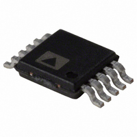
AD5443YRMZ-REEL7 Analog Devices Inc, AD5443YRMZ-REEL7 Datasheet - Page 5

AD5443YRMZ-REEL7
Manufacturer Part Number
AD5443YRMZ-REEL7
Description
IC,D/A CONVERTER,SINGLE,12-BIT,CMOS,TSSOP,10PIN
Manufacturer
Analog Devices Inc
Datasheet
1.AD5443YRMZ.pdf
(28 pages)
Specifications of AD5443YRMZ-REEL7
Design Resources
Unipolar, Precision DC Digital-to-Analog Conversion Using AD5426/32/43 8-Bit to12-Bit DACs (CN0034) Precision, Bipolar Configuration for the AD5426/32/43 8-Bit to12-Bit DACs (CN0036) AC Signal Processing Using AD5426/32/43 Current Output DACs (CN0037) Programmable Gain Element Using AD5426/32/43 Current Output DACs (CN0038) Single-Ended-to-Differential Converters for Voltage Output and Current Output DACs Using AD8042 (CN0143)
Number Of Bits
12
Data Interface
Serial
Number Of Converters
1
Voltage Supply Source
Single Supply
Operating Temperature
-40°C ~ 125°C
Mounting Type
Surface Mount
Package / Case
10-MSOP, Micro10™, 10-uMAX, 10-uSOP
Power Dissipation (max)
25µW
Settling Time
50ns
Lead Free Status / RoHS Status
Lead free / RoHS Compliant
For Use With
EVAL-AD5443-DBRDZ - BOARD EVAL CARD CLINUX/STAMP
Lead Free Status / RoHS Status
Lead free / RoHS Compliant
Available stocks
Company
Part Number
Manufacturer
Quantity
Price
Company:
Part Number:
AD5443YRMZ-REEL7
Manufacturer:
ST
Quantity:
934
TIMING CHARACTERISTICS
All input signals are specified with tr = tf = 1 ns (10% to 90% of V
V
Table 2.
Parameter
f
t
t
t
t
t
t
t
t
t
1
2
SCLK
1
2
3
4
5
6
7
8
9
Falling or rising edge as determined by control bits of serial word.
Daisy-chain and readback modes cannot operate at maximum clock frequency. SDO timing specifications measured with load circuit, as shown in Figure 4.
1
2
REF
= 10 V, I
SCLK
SYNC
SYNC
SDIN
SCLK
SDO
DIN
ALTERNATIVELY, DATA MAY BE CLOCKED INTO INPUT SHIFT REGISTER ON RISING EDGE OF
SCLK AS DETERMINED BY CONTROL BITS. TIMING AS PER ABOVE, WITH SCLK INVERTED.
ALTERNATIVELY, DATA MAY BE CLOCKED INTO INPUT SHIFT REGISTER ON RISING EDGE OF SCLK AS
DETERMINED BY CONTROL BITS. IN THIS CASE, DATA WOULD BE CLOCKED OUT OF SDO ON FALLING
EDGE OF SCLK. TIMING AS PER ABOVE, WITH SCLK INVERTED.
OUT
2 = 0 V; temperature range for Y version: −40°C to +125°C; all specifications T
2.5 V to 5.5 V
50
20
8
8
13
5
3
5
30
80
120
t
8
t
4
t
DB15 (N)
4
DB15
t
5
t
5
t
t6
6
4.5 V to 5.5 V
50
20
8
8
13
5
3
5
30
45
65
t
6
Figure 3. Daisy-Chain and Readback Modes Timing Diagram
t
2
Figure 2. Standalone Mode Timing Diagram
t
2
Unit
MHz max
ns min
ns min
ns min
ns min
ns typ
ns min
ns min
ns min
ns min
ns max
t
1
t
3
Rev. C | Page 5 of 28
t
1
t
3
DB0 (N)
DD
) and timed from a voltage level of (V
t
9
DB0
DB15(N)
t
(N + 1)
7
DB15
Conditions/Comments
Max clock frequency
SCLK cycle time
SCLK high time
SCLK low time
SYNC falling edge to SCLK active edge setup time
Data setup time
Data hold time
SYNC rising edge to SCLK active edge
Minimum SYNC high time
SCLK active edge to SDO valid
MIN
to T
AD5426/AD5432/AD5443
MAX
IL
, unless otherwise noted.
+ V
IH
DB0(N)
)/2. V
(N + 1)
DB0
t
7
DD
= 2.5 V to 5.5 V,
t
8


