AD5384BBC-3 Analog Devices Inc, AD5384BBC-3 Datasheet
AD5384BBC-3
Specifications of AD5384BBC-3
Available stocks


Related parts for AD5384BBC-3


AD5384BBC-3 Summary of contents
Page 1
FEATURES Guaranteed monotonic INL error: ±4 LSB max On-chip 1.25 V/2 ppm/°C reference Temperature range: –40°C to +85°C Rail-to-rail output amplifier Power-down Package type: 100-lead CSPBGA (10 mm × 10 mm) User Interfaces: Serial (SPI-®/QSPI-™/MICROWIRE-™/DSP-compatible, featuring data readback) ...
Page 2
AD5384 TABLE OF CONTENTS General Description ......................................................................... 3 Specifications..................................................................................... 4 AD5384-5 Specifications ............................................................. 4 AC Characteristics........................................................................ 6 AD5384-3 Specifications ............................................................. 7 AC Characteristics........................................................................ 9 Timing Characteristics................................................................... 10 Serial Interface ............................................................................ Serial Interface...................................................................... 12 Absolute Maximum Ratings.......................................................... ...
Page 3
... Table 1. Complete Family of High Channel Count, Low Voltage, Single-Supply DACs in Portfolio Model Resolution AV Range DD AD5380BST-5 14 Bits 4 5.5 V AD5380BST-3 14 Bits 2 3.6 V AD5381BST-5 12 Bits 4 5.5 V AD5381BST-3 12 Bits 2 3.6 V AD5384BBC-5 14 Bits 4 5.5 V AD5384BBC-3 14 Bits 2 3.6 V AD5382BST-5 14 Bits 4 5.5 V AD5382BST-3 14 Bits 2 3.6 V AD5383BST-5 12 Bits 4 5.5 V AD5383BST-3 12 Bits 2 3.6 V AD5390BST-5 14 Bits 4 5.5 V AD5390BCP-5 14 Bits 4 5.5 V ...
Page 4
AD5384 SPECIFICATIONS AD5384-5 SPECIFICATIONS 5.5 V, AGND = DGND = 0 V; external REFIN = 2.5 V; all specifications otherwise noted. Table 3. Parameter ACCURACY ...
Page 5
Parameter 3 LOGIC OUTPUTS (BUSY, SDO Output Low Voltage Output High Voltage Output Low Voltage Output High Voltage OH High Impedance Leakage Current High Impedance Output Capacitance 3 LOGIC ...
Page 6
AD5384 1 AC CHARACTERISTICS 5.5 V, AGND = DGND = Table 4. Parameter DYNAMIC PERFORMANCE Output Voltage Settling Time Slew Rate 2 Digital-to-Analog Glitch ...
Page 7
AD5384-3 SPECIFICATIONS 5.5 V, AGND = DGND = 0 V; external REFIN = 1.25 V; all specifications unless otherwise noted. Table 5. Parameter ACCURACY Resolution ...
Page 8
AD5384 Parameter 3 LOGIC OUTPUTS (BUSY, SDO Output Low Voltage Output High Voltage OH High Impedance Leakage Current High Impedance Output Capacitance LOGIC OUTPUT (SDA Output Low Voltage OL Three-State Leakage Current ...
Page 9
AC CHARACTERISTICS 3.6 V and 4 5 Table 6. Parameter DYNAMIC PERFORMANCE Output Voltage Settling Time Slew Rate 2 Digital-to-Analog Glitch Energy Glitch Impulse Peak Amplitude Channel-to-Channel Isolation DAC-to-DAC ...
Page 10
AD5384 TIMING CHARACTERISTICS SERIAL INTERFACE 3.6 V; AGND = DGND = 0 V; all specifications unless otherwise noted. Table ...
Page 11
SCLK SYNC DIN DB23 BUSY 1 LDAC 1 V OUT 2 LDAC 2 V OUT t 18 CLR V OUT 1 LDAC ACTIVE DURING BUSY 2 LDAC ...
Page 12
AD5384 SERIAL INTERFACE 3.6 V; AGND = DGND = 0 V; all specifications unless otherwise noted. ...
Page 13
ABSOLUTE MAXIMUM RATINGS 25°C, unless otherwise noted. A Table 9. Parameter Rating AV to AGND –0 DGND –0 Digital Inputs to DGND –0 ...
Page 14
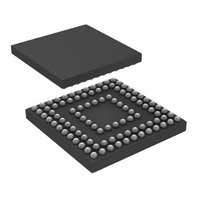
AD5384 PIN CONFIGURATION AND FUNCTION DESCRIPTIONS Table 10. Pin Number and Name CSPBGA Ball CSPBGA Ball Number Name Number Name RESET A2 VOUT24 B10 VOUT22 A3 B11 NC CLR A4 SYNC B12 VOUT23 A5 SCLK C1 VOUT26 ...
Page 15
Table 11. Pin Function Descriptions Mnemonic Function VOUTx Buffered Analog Outputs for Channel x. Each analog output is driven by a rail-to-rail output amplifier operating at a gain of 2. Each output is capable of driving an output load of ...
Page 16
AD5384 Mnemonic Function PD Power Down (Level Sensitive, Active High used to place the device in low power mode, where AI 2 µA and µA. In power-down mode, all internal analog circuitry is placed in ...
Page 17
TERMINOLOGY Relative Accuracy Relative accuracy or endpoint linearity is a measure of the maximum deviation from a straight line passing through the endpoints of the DAC transfer function measured after adjusting for zero-scale error and full-scale error, and ...
Page 18
AD5384 TYPICAL PERFORMANCE CHARACTERISTICS 2.0 1.5 1.0 0.5 0 –0.5 –1.0 –1.5 –2.0 0 4096 8192 INPUT CODE Figure 8. Typical AD5384-5 INL Plot 2.539 2.538 V = 2.5V REF 2.537 T = ...
Page 19
AI (mA) DD Figure 14. Histogram with Boost Off 0.4 0.5 0.6 0.7 0.8 DI (mA) DD Figure 15. DI Histogram DD WR BUSY ...
Page 20
AD5384 6 FULL-SCALE 5 AV 3/4 SCALE 4 MIDSCALE 3 2 1/4 SCALE 1 ZERO-SCALE 0 –1 –40 –20 –10 –5 – CURRENT (mA) Figure 20. AD5384-5 Output Amplifier Source and Sink Capability 0.20 0.15 0.10 ERROR AT ...
Page 21
FUNCTIONAL DESCRIPTION DAC ARCHITECTURE—GENERAL The AD5384 is a complete single-supply, 40-channel, voltage output DAC offering 14-bit resolution, available in a 100-lead CSPBGA package. It features two serial interfaces, SPI and I This family includes an internal1.25/2 ppm/°C reference ...
Page 22
AD5384 Table 15. Gain Data Format (REG1 = 0, REG0 = 1) DB13 to DB0 11 1111 1111 1110 10 1111 1111 1110 01 1111 1111 1110 00 1111 1111 1110 00 0000 0000 0000 ON-CHIP SPECIAL FUNCTION REGISTERS (SFR) ...
Page 23
Table 17. Control Register Contents MSB CR13 CR12 CR11 CR10 Control Register Write/Read REG1 = REG0 = 0, A5–A0 = 001100 status determines if the operation is a write ( read (R/ W ...
Page 24
AD5384 Table 19. AD5384 Channel Monitor Decoding REG1 REG0 ...
Page 25
HARDWARE FUNCTIONS RESET FUNCTION Bringing the RESET line low resets the contents of all internal registers to their power-on reset state. Reset is a negative edge- sensitive input. The default corresponds full scale and ...
Page 26
AD5384 INTERFACES The AD5384 contains a serial interface that can be programmed either as DSP-, SPI-, MICROWIRE compatible. The SPI/ I2C pin is used to select DSP, SPI, 2 MICROWIRE interface mode. To minimize both ...
Page 27
Daisy-Chain Mode For systems that contain several devices, the SDO pin can be used to daisy-chain several devices together. This daisy-chain mode can be useful in system diagnostics and in reducing the number of serial interface lines. By connecting DCEN ...
Page 28
AD5384 SERIAL INTERFACE 2 The AD5384 features an I C-compatible 2-wire interface consisting of a serial data line (SDA) and a serial clock line (SCL). SDA and SCL facilitate communication between the AD5384 and the master at ...
Page 29
SCL SDA START COND BY MASTER ADDRESS BYTE SCL REG1 REG0 MSB SDA MOST SIGNIFICANT BYTE SCL SDA START COND BY MASTER ADDRESS BYTE SCL SDA REG1 REG0 MSB MOST ...
Page 30
AD5384 2-Byte Mode Following initialization of 2-byte mode, the user can update channels sequentially. The device address byte is required only once, and the pointer address pointer is configured for auto- increment or burst mode. The user must begin with ...
Page 31
MICROPROCESSOR INTERFACING AD5384 to MC68HC11 The serial peripheral interface (SPI) on the MC68HC11 is configured for master mode (MSTR = 1), the Clock Polarity bit (CPOL and the Clock Phase bit (CPHA The SPI is configured ...
Page 32
AD5384 APPLICATION INFORMATION POWER SUPPLY DECOUPLING In any circuit where accuracy is important, careful considera- tion of the power supply and ground return layout helps to ensure the rated performance. The printed circuit board on which the AD5384 is mounted ...
Page 33
Each of the 40 DAC channels on the AD5384 contains an A and B data register. Note that the B registers can be loaded only when toggle mode is enabled. The sequence of events when configuring the AD5384 for toggle ...
Page 34
AD5384 OPTICAL ATTENUATORS Based on its high channel count, high resolution, monotonic behavior, and high level of integration, the AD5384 is ideally targeted at optical attenuation applications used in dynamic gain equalizers, variable optical attenuators (VOA), and optical add-drop multiplexers ...
Page 35
... ORDERING GUIDE Model Resolution Temperature Range AD5384BBC-5 14 Bits –40°C to +85°C AD5384BBC-5REEL7 14 Bits –40°C to +85°C AD5384BBC-3 14 Bits –40°C to +85°C AD5384BBC-3REEL7 14 Bits –40°C to +85°C 10.00 BSC BALL A1 PAD CORNER 8.80 BSC TOP VIEW DETAIL A DETAILA ...
Page 36
AD5384 NOTES 2 Purchase of licensed I C components of Analog Devices or one of its sublicensed Associated Companies conveys a license for the purchaser under the Philips I 2 Rights to use these components system, ...