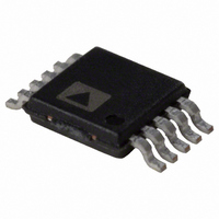
AD5325ARMZ-REEL7 Analog Devices Inc, AD5325ARMZ-REEL7 Datasheet - Page 18

AD5325ARMZ-REEL7
Manufacturer Part Number
AD5325ARMZ-REEL7
Description
12-BIT QUAD I2C DAC I.C.
Manufacturer
Analog Devices Inc
Datasheet
1.AD5305ARMZ.pdf
(24 pages)
Specifications of AD5325ARMZ-REEL7
Settling Time
6µs
Number Of Bits
12
Data Interface
I²C, Serial
Number Of Converters
4
Voltage Supply Source
Single Supply
Power Dissipation (max)
5mW
Operating Temperature
-40°C ~ 105°C
Mounting Type
Surface Mount
Package / Case
10-MSOP, Micro10™, 10-uMAX, 10-uSOP
Lead Free Status / RoHS Status
Lead free / RoHS Compliant
AD5305/AD5315/AD5325
DOUBLE-BUFFERED INTERFACE
The AD5305/AD5315/AD5325 DACs have double-buffered
interfaces consisting of two banks of registers—input registers
and DAC registers. The input register is directly connected to the
input shift register and the digital code is transferred to the relevant
input register on completion of a valid write sequence. The DAC
register contains the digital code used by the resistor string.
Access to the DAC register is controlled by the LDAC bit. When
the LDAC bit is set high, the DAC register is latched and,
therefore, the input register can change state without affecting
the contents of the DAC register. However, when the LDAC bit
is set low, the DAC register becomes transparent and the
contents of the input register are transferred to it.
This is useful if the user requires simultaneous updating of all
DAC outputs. The user can write to three of the input registers
individually and then, by setting the LDAC bit low when
writing to the remaining DAC input register, all outputs update
simultaneously.
SDA
SDA
SDA
SCL
SCL
SCL
NOTE: DATA BYTES ARE THE SAME AS THOSE IN THE WRITE SEQUENCE EXCEPT THAT DON’T CARES ARE READ BACK AS 0s.
MASTER
START
COND
BY
REPEATED
MASTER
START
COND
0
BY
MSB
0
0
0
0
LEAST SIGNIFICANT DATA BYTE
ADDRESS BYTE
ADDRESS BYTE
0
1
1
1
0
1
A0
0
Figure 34. Readback Sequence
A0
R/W
LSB
AD53x5
Rev. G | Page 18 of 24
ACK
BY
R/W
MASTER
ACK
NO
BY
MSB
AD53x5
X
ACK
BY
MASTER
COND
STOP
These parts contain an extra feature whereby the DAC register
is not updated unless its input register has been updated since
the last time that LDAC was brought low. Normally, when
LDAC is brought low, the DAC registers are filled with the
contents of the input registers. In the case of the AD5305/AD5315/
AD5325, the part updates the DAC register only if the input
register has been changed since the last time the DAC register
was updated, thereby removing unnecessary digital crosstalk.
POWER-DOWN MODES
The AD5305/AD5315/AD5325 have very low power consumption,
dissipating typically 1.5 mW with a 3 V supply and 3 mW with
a 5 V supply. Power consumption can be further reduced when
the DACs are not in use by putting them into one of three
power-down modes, which are selected by Bit 15 and Bit 14
(PD1 and PD0) of the data byte. Table 8 shows how the state of
the bits corresponds to the mode of operation of the DAC.
Table 8. PD1/PD0 Operating Modes
PD1
0
0
1
1
BY
X
MSB
PD0
0
1
0
1
POINTER BYTE
Operating Mode
Normal Operation
Power-Down (1 kΩ load to GND)
Power-Down (100 kΩ load to GND)
Power-Down (three-state output)
DATA BYTE
LSB
AD53x5
ACK
BY
LSB
MASTER
ACK
BY


