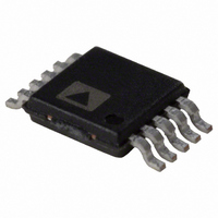
AD5312BRM Analog Devices Inc, AD5312BRM Datasheet - Page 12

AD5312BRM
Manufacturer Part Number
AD5312BRM
Description
D/A Converter (D-A) IC
Manufacturer
Analog Devices Inc
Datasheet
1.AD5302ARMZ.pdf
(24 pages)
Specifications of AD5312BRM
Digital Ic Case Style
MSOP
No. Of Pins
10
Operating Temperature Range
-40°C To +105°C
Peak Reflow Compatible (260 C)
No
No. Of Bits
10 Bit
Leaded Process Compatible
No
Mounting Type
Surface Mount
Rohs Status
RoHS non-compliant
Settling Time
6µs
Number Of Bits
10
Data Interface
Serial
Number Of Converters
2
Voltage Supply Source
Single Supply
Power Dissipation (max)
2.5mW
Operating Temperature
-40°C ~ 105°C
Package / Case
10-MSOP, Micro10™, 10-uMAX, 10-uSOP
Lead Free Status / RoHS Status
Contains lead / RoHS non-compliant
Available stocks
Company
Part Number
Manufacturer
Quantity
Price
Part Number:
AD5312BRM
Manufacturer:
ADI/亚德诺
Quantity:
20 000
Company:
Part Number:
AD5312BRM-REEL7
Manufacturer:
AD
Quantity:
5 510
Company:
Part Number:
AD5312BRM-REEL7
Manufacturer:
SIEMENS
Quantity:
5 510
Part Number:
AD5312BRMZ
Manufacturer:
ADI/亚德诺
Quantity:
20 000
AD5302/AD5312/AD5322
600
500
400
300
200
100
700
600
500
400
300
200
100
1.0
0.8
0.6
0.4
0.2
0
0
2.5
2.7
0
BOTH DACS IN
THREE-STATE CONDITION
Figure 19. Power-Down Current vs. Supply Voltage
BOTH DACS IN GAIN-OF-TWO MODE
REFERENCE INPUTS BUFFERED
T
A
Figure 18. Supply Current vs. Supply Voltage
0.5
=
Figure 20. Supply vs. Logic Input Voltage
25°C
3.0
3.2
1.0
1.5
–40°C
3.5
V
3.7
DD
2.0
= 3V
V
V
LOGIC
V
+25°C
DD
DD
4.0
2.5
(V)
4.2
(V)
(V)
+105°C
3.0
+25°C
4.5
V
3.5
DD
–
4.7
40
= 5V
°C
4.0
+105°C
5.0
5.2
4.5
5.5
5.0
Rev. C | Page 12 of 24
CH2
CH1
CH1
CH2
CH1
CH3
Figure 21. Half-Scale Setting (¼ to ¾ Scale Code Change)
T
T
A
A
CLK
=
=
Figure 23. Existing Power-Down to Midscale
25°C
25°C
CH1 1V, CH2 1V, TIME BASE = 20µs/DIV
V
CH1 1V, CH3 5V, TIME BASE = 1µs/DIV
CH1 1V, CH2 5V, TIME BASE = 5µs/DIV
Figure 22. Power-On Reset to 0 V
OUT
CLK
V
OUT
V
DD
V
OUT
A
V
T
DD
A
=
= 5V
25°C


