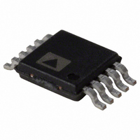
AD5302BRMZ Analog Devices Inc, AD5302BRMZ Datasheet - Page 16

AD5302BRMZ
Manufacturer Part Number
AD5302BRMZ
Description
IC,D/A CONVERTER,DUAL,8-BIT,CMOS,TSSOP,10PIN
Manufacturer
Analog Devices Inc
Datasheet
1.AD5302ARMZ.pdf
(24 pages)
Specifications of AD5302BRMZ
Settling Time
6µs
Number Of Bits
8
Data Interface
Serial
Number Of Converters
2
Voltage Supply Source
Single Supply
Power Dissipation (max)
2.5mW
Operating Temperature
-40°C ~ 105°C
Mounting Type
Surface Mount
Package / Case
10-MSOP, Micro10™, 10-uMAX, 10-uSOP
Number Of Channels
2
Resolution
8b
Conversion Rate
167KSPS
Interface Type
Serial (3-Wire, SPI, QSPI, Microwire)
Single Supply Voltage (typ)
3.3/5V
Dual Supply Voltage (typ)
Not RequiredV
Architecture
Resistor-String
Power Supply Requirement
Single
Output Type
Voltage
Integral Nonlinearity Error
±0.5LSB
Single Supply Voltage (min)
2.5V
Single Supply Voltage (max)
5.5V
Dual Supply Voltage (min)
Not RequiredV
Dual Supply Voltage (max)
Not RequiredV
Operating Temp Range
-40C to 105C
Operating Temperature Classification
Industrial
Mounting
Surface Mount
Pin Count
10
Package Type
MSOP
Lead Free Status / RoHS Status
Lead free / RoHS Compliant
Lead Free Status / RoHS Status
Lead free / RoHS Compliant
Available stocks
Company
Part Number
Manufacturer
Quantity
Price
Part Number:
AD5302BRMZ
Manufacturer:
ADI/亚德诺
Quantity:
20 000
Company:
Part Number:
AD5302BRMZ-REEL7
Manufacturer:
AD
Quantity:
4 500
AD5302/AD5312/AD5322
POWER-DOWN MODES
The AD5302/AD5312/AD5322 have very low power consump-
tion, dissipating only 0.7 mW with a 3 V supply and 1.5 mW
with a 5 V supply. Power consumption can be further reduced
when the DACs are not in use by putting them into one of three
power-down modes, which are selected by Bit 13 and Bit 12
(PD1 and PD0) of the control word. Table 7 shows how the
state of the bits corresponds to the mode of operation of that
particular DAC.
Table 7. PD1/PD0 Operating Modes
PD1
0
0
1
1
When both bits are set to 0, the DACs work normally with
their normal power consumption of 300 μA at 5 V. However,
for the three power-down modes, the supply current falls to
200 nA at 5 V (50 nA at 3 V). Not only does the supply current
drop, but the output stage is also internally switched from the
output of the amplifier to a resistor network of known values.
This has the advantage that the output impedance of the part is
known while the part is in power-down mode and provides a
defined input condition for whatever is connected to the output
of the DAC amplifier. There are three different options.
PDO
0
1
0
1
Operating Mode
Normal Operation
Power-Down (1 kΩ Load to GND)
Power-Down (100 kΩ Load to GND)
Power-Down (High Impedance Output)
Rev. C | Page 16 of 24
•
•
•
The output stage is illustrated in Figure 33.
The bias generator, the output amplifier, the resistor string,
and all other associated linear circuitry are shut down when
the power-down mode is activated. However, the contents of
the registers are unaffected when in power-down. The time to
exit power-down is typically 2.5 μs for V
V
DD
= 3 V. See Figure 23 for a plot.
The output is connected internally to GND through a
1 kΩ resistor,
The output is connected internally to GND through a
100 kΩ resistor, or
The output is left open-circuited (three-state).
STRING DAC
RESISTOR-
Figure 33. Output Stage During Power-Down
POWER-DOWN
CIRCUITRY
AMPLIFIER
DD
= 5 V and 5 μs when
RESISTOR
NETWORK
V
OUT


