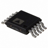
AD5271BRMZ-20-RL7 Analog Devices Inc, AD5271BRMZ-20-RL7 Datasheet - Page 7

AD5271BRMZ-20-RL7
Manufacturer Part Number
AD5271BRMZ-20-RL7
Description
256 Tap 5v 50tp, 1% R-tol MSOP SPI I.C.
Manufacturer
Analog Devices Inc
Datasheet
1.AD5271BRMZ-20.pdf
(24 pages)
Specifications of AD5271BRMZ-20-RL7
Taps
256
Resistance (ohms)
20K
Number Of Circuits
1
Temperature Coefficient
5ppm/°C
Memory Type
Non-Volatile
Interface
SPI Serial
Voltage - Supply
±2.5 V ~ ±2.75 V, 2.7 V ~ 5.5 V
Operating Temperature
-40°C ~ 125°C
Mounting Type
Surface Mount
Package / Case
10-MSOP, Micro10™, 10-uMAX, 10-uSOP
Resistance In Ohms
*
Lead Free Status / RoHS Status
Lead free / RoHS Compliant
INTERFACE TIMING SPECIFICATIONS
V
Table 7.
Parameter
t
t
t
t
t
t
t
t
t
t
t
t
t
t
t
t
1
2
3
4
5
6
Shift Register and Timing Diagrams
SYNC
SCLK
1
2
3
4
5
6
7
8
9
10
RDAC_R-PERF
RDAC_NORMAL
MEMORY_READ
MEMORY_PROGRAM
RESET
POWER-UP
All input signals are specified with tr = tf = 1 ns/V (10% to 90% of V
Maximum SCLK frequency is 50 MHz.
Refer to t
Refer to t
R
Maximum time after V
SDO
2
3, 4
DIN
DD
PULL_UP
5
= 2.5 V to 5.5 V, V
= 2.2 kΩ to V
6
RDAC_R-PER
MEMORY_READ
t
8
and t
t
4
and t
DD
0
DD
RDAC_NORMAL
with a capacitance load of 168 pF.
MEMORY_PROGRAM
− V
SS
Limit
20
10
10
15
5
5
1
500
15
450
2
600
6
350
0.6
2
SS
0
t
= 0 V; V
2
0
is equal to 2.5 V.
for RDAC register write operations.
t
3
1
0
for memory commands operations.
C3
DD
C3
= 2.5 V, V
Unit
ns min
ns min
ns min
ns min
ns min
ns min
ns min
ns min
ns min
ns max
μs max
ns max
μs max
ms max
ms max
ms max
t
1
CONTROL BITS
C2
C2
SS
C1
Figure 3. Write Timing Diagram (CPOL = 0, CPHA = 1)
= −2.5 V; all specifications T
C0
Test Conditions/Comments
SCLK cycle time
SCLK high time
SCLK low time
SYNC to SCLK falling edge setup time
Data setup time
Data hold time
SCLK falling edge to SYNC rising edge
Minimum SYNC high time
SYNC rising edge to next SCLK fall ignored
SCLK rising edge to SDO valid
RDAC register write command execute time
RDAC register write command execute time
Memory readback execute time
Memory program time
Reset 50-TP restore time
Power-on 50-TP restore time
D7
DD
DB9 (MSB)
Figure 2. Shift Register Content
) and timed from a voltage level of (V
D9
Rev. E | Page 7 of 24
D6
D8
D7
D5
D6
MIN
DATA BITS
to T
D5
MAX
D4
D2
, unless otherwise noted.
IL
+ V
D3
IH
)/2.
t
D1
5
t
D2
6
D0
D1
t
7
DB0 (LSB)
t
9
D0
AD5270/AD5271


