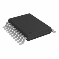
AD5253BRUZ50 Analog Devices Inc, AD5253BRUZ50 Datasheet - Page 23

AD5253BRUZ50
Manufacturer Part Number
AD5253BRUZ50
Description
IC,Digital Potentiometer,CMOS,TSSOP,20PIN,PLASTIC
Manufacturer
Analog Devices Inc
Datasheet
1.AD5254BRUZ100.pdf
(32 pages)
Specifications of AD5253BRUZ50
Taps
64
Resistance (ohms)
50K
Number Of Circuits
4
Temperature Coefficient
650 ppm/°C Typical
Memory Type
Non-Volatile
Interface
I²C, 2-Wire Serial
Voltage - Supply
2.7 V ~ 5.5 V, ±2.25 V ~ 2.75 V
Operating Temperature
-40°C ~ 85°C
Mounting Type
Surface Mount
Package / Case
20-TSSOP
Resistance In Ohms
50K
Number Of Elements
4
# Of Taps
64
Resistance (max)
50KOhm
Power Supply Requirement
Single/Dual
Interface Type
Serial (2-Wire/I2C)
Single Supply Voltage (typ)
3/5V
Dual Supply Voltage (typ)
±2.5V
Single Supply Voltage (min)
2.7V
Single Supply Voltage (max)
5.5V
Dual Supply Voltage (min)
±2.25V
Dual Supply Voltage (max)
±2.75V
Operating Temp Range
-40C to 85C
Operating Temperature Classification
Industrial
Mounting
Surface Mount
Pin Count
20
Lead Free Status / RoHS Status
Lead free / RoHS Compliant
Lead Free Status / RoHS Status
Lead free / RoHS Compliant
Available stocks
Company
Part Number
Manufacturer
Quantity
Price
Part Number:
AD5253BRUZ50
Manufacturer:
ADI/亚德诺
Quantity:
20 000
Company:
Part Number:
AD5253BRUZ50-RL7
Manufacturer:
RENESAS
Quantity:
13 400
TERMINAL VOLTAGE OPERATION RANGE
The AD5253/AD5254 are designed with internal ESD diodes
for protection; these diodes also set the boundaries for the
terminal operating voltages. Positive signals present on
Terminal A, Terminal B, or Terminal W that exceed V
clamped by the forward-biased diode. Similarly, negative signals
on Terminal A, Terminal B, or Terminal W that are more
negative than V
users should not operate V
the voltage across V
polarity constraint.
2
Figure 38. Four Devices with AD1 and AD0 of 00
2 × 4
DECODER
2 × 4
DECODER
2 × 4
DECODER
2 × 4
DECODER
SS
are also clamped (see Figure 39). In practice,
DD
to V
4
4
4
4
AB
SS
, but V
, V
WA
, and V
N1
N2
AB
P4
R1
R2
X
, V
R3
P3
R4
X
+5V
WA
X
+5V
X
+5V
+5V
WB
, and V
P2
to be higher than
Y
P2
N3
Y
+5
× 4
R3
Y
× 4
× 4
× 4
Y
WB
have no
AD1
AD0
DD
AD1
AD0
AD1
AD0
AD1
AD0
are
Rev. B | Page 23 of 32
POWER-UP AND POWER-DOWN SEQUENCES
Because the ESD protection diodes limit the voltage compliance
at Terminal A, Terminal B, and Terminal W (Figure 39), it is
important to power V
these terminals. Otherwise, the diodes are forward biased such
that V
user’s circuit. Similarly, V
The ideal power-up sequence is in the following order: GND,
V
V
they are powered after V
LAYOUT AND POWER SUPPLY BIASING
It is always a good practice to employ a compact, minimum
lead-length layout design. The leads to the input should be as
direct as possible, with a minimum conductor length. Ground
paths should have low resistance and low inductance.
Similarly, it is also good practice to bypass the power supplies
with quality capacitors. Low equivalent series resistance (ESR)
1 μF to 10 μF tantalum or electrolytic capacitors should be
applied at the supplies to minimize any transient disturbance
and filter low frequency ripple. Figure 40 illustrates the basic
supply-bypassing configuration for the AD5253/AD5254.
The ground pin of the AD5253/AD5254 is used primarily as a
digital ground reference. To minimize the digital ground
bounce, the AD5253/AD5254 ground terminal should be joined
remotely to the common ground (see Figure 40).
DD
A
, V
, V
B
DD
, V
SS
Figure 39. Maximum Terminal Voltages Set by V
/V
, digital inputs, and V
W
V
V
SS
DD
, and the digital inputs is not important, as long as
SS
Figure 40. Power Supply-Bypassing Configuration
are powered unintentionally and may affect the
C3
C4
10μF
10μF
C1
C2
DD
0.1μF
0.1μF
/V
DD
DD
SS
/V
/V
before applying any voltage to
SS
A
SS
/V
.
should be powered down last.
AD5253/AD5254
V
V
B
DD
SS
/V
W
. The order of powering
AD5253/AD5254
GND
V
A
W
B
V
DD
SS
DD
and V
SS


