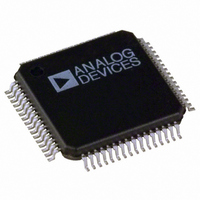
AD1937WBSTZ Analog Devices Inc, AD1937WBSTZ Datasheet - Page 18

AD1937WBSTZ
Manufacturer Part Number
AD1937WBSTZ
Description
4ADCs/8DACs W/PLL 192 KHz, 24Bt Codec
Manufacturer
Analog Devices Inc
Type
General Purposer
Datasheet
1.AD1937WBSTZ.pdf
(36 pages)
Specifications of AD1937WBSTZ
Data Interface
Serial
Resolution (bits)
24 b
Number Of Adcs / Dacs
4 / 8
Sigma Delta
Yes
S/n Ratio, Adcs / Dacs (db) Typ
96 / 96
Dynamic Range, Adcs / Dacs (db) Typ
105 / 110
Voltage - Supply, Analog
3 V ~ 3.6 V
Voltage - Supply, Digital
3 V ~ 3.6 V
Operating Temperature
-40°C ~ 125°C
Mounting Type
Surface Mount
Package / Case
64-LQFP
Lead Free Status / RoHS Status
Lead free / RoHS Compliant
Available stocks
Company
Part Number
Manufacturer
Quantity
Price
Company:
Part Number:
AD1937WBSTZ
Manufacturer:
ADI
Quantity:
210
Company:
Part Number:
AD1937WBSTZ
Manufacturer:
Analog Devices Inc
Quantity:
10 000
Part Number:
AD1937WBSTZ
Manufacturer:
ADI/亚德诺
Quantity:
20 000
Company:
Part Number:
AD1937WBSTZ-RL
Manufacturer:
Analog Devices Inc
Quantity:
10 000
Part Number:
AD1937WBSTZ-RL
Manufacturer:
ADI/亚德诺
Quantity:
20 000
AD1937
Table 13. I
Abbreviation
S
P
AM
AS
Table 14. Single Word I
S
Table 15. Burst Mode I
S
Table 16. Single Word I
S
Table 17. Burst Mode I
S
POWER SUPPLY AND VOLTAGE REFERENCE
The AD1937 is designed for a 3.3 V supply. Separate power
supply pins are provided for the analog and digital sections.
To minimize noise pickup, these pins should be bypassed with
100 nF ceramic chip capacitors placed as close to the pins as
possible. A bulk aluminum electrolytic capacitor of at least
22 μF should also be provided on the same printed circuit
board (PCB) as the codec. For critical applications, improved
performance is obtained with separate supplies for the analog
and digital sections. If this is not possible, it is recommended
that the analog and digital load pins be isolated by means of a
ferrite bead in series with the supply. It is important that the
analog supply be as clean as possible.
The AD1937 includes a 3.3 V regulator driver that only requires
an external pass transistor, a resistor, and bypass capacitors to
turn a 5 V supply into 3.3 V. If the regulator driver is not used,
connect VSUPPLY, VDRIVE, and VSENSE to DGND.
All digital inputs are compatible with TTL and CMOS levels.
All outputs are driven from the 3.3 V DVDD supply and are
compatible with TTL and 3.3 V CMOS levels.
Chip Address,
R/W = 0
Chip Address, R/W = 0
Chip Address, R/W = 0
Chip Address, R/W = 0
2
C Abbreviation Table
AS
2
2
C Write
C Read
2
2
C Write
C Read
Register
Address
AS
AS
Register Address
Register Address
AS
AS
S
Condition
Repeated start by master
Stop by master
Acknowledge by master
Acknowledge by AD1937
Chip Address,
R/W = 1
Register Address
AS
Rev. B | Page 18 of 36
AS
Data Word 1
S
The ADC and DAC internal analog voltage reference (V
brought out on the FILTR pin and should be bypassed as close
as possible to the chip with a parallel combination of 10 μF and
100 nF capacitors. Any external current drawn should be limited
to less than 50 μA.
The internal reference can be disabled in the PLL and Clock
Control 1 register, and FILTR can be driven from an external
source. This can be used to scale the DAC output to the clipping
level of a power amplifier based on its power supply voltage.
The ADC input gain varies by the inverse ratio. It is not advisable
to drive the FILTR pin with more than (AVDD/2) V. The total
gain from ADC input to DAC output remains constant.
The CM pin should be bypassed as close as possible to the chip,
with a parallel combination of 47 μF and 100 nF capacitors. This
voltage can be used to bias external op amps to the common-mode
voltage of the input and output signal pins. The output current
should be limited to less than 0.5 mA source and 2 mA sink.
AS
Chip Address, R/W = 1
Data
Word 1
AS
Data Word 2
AS
AM
Data
Word 2
Data Word
AS
AS
AM
Data Word
Data Word N
Data
Word N
AS
AM
REF
AS
AM
) is
P
P
P
P


