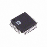
AD1833AASTZ Analog Devices Inc, AD1833AASTZ Datasheet - Page 5

AD1833AASTZ
Manufacturer Part Number
AD1833AASTZ
Description
6 Channel 24 Bit 192 KHz DAC I.C.
Manufacturer
Analog Devices Inc
Datasheet
1.AD1833ACSTZ.pdf
(20 pages)
Specifications of AD1833AASTZ
Number Of Bits
24
Data Interface
DSP, I²S, Serial
Number Of Converters
6
Voltage Supply Source
Analog and Digital
Operating Temperature
-40°C ~ 85°C
Mounting Type
Surface Mount
Package / Case
48-LQFP
Lead Free Status / RoHS Status
Lead free / RoHS Compliant
Power Dissipation (max)
-
Settling Time
-
Lead Free Status / RoHS Status
Lead free / RoHS Compliant
Available stocks
Company
Part Number
Manufacturer
Quantity
Price
Company:
Part Number:
AD1833AASTZ
Manufacturer:
Analog Devices Inc
Quantity:
10 000
Company:
Part Number:
AD1833AASTZ-REEL
Manufacturer:
Analog Devices Inc
Quantity:
10 000
AUXL/RCLK
CAUTION
ESD (electrostatic discharge) sensitive device. Electrostatic charges as high as 4000 V readily accumulate
on the human body and test equipment and can discharge without detection. Although the AD1833A
features proprietary ESD protection circuitry, permanent damage may occur on devices subjected to
high energy electrostatic discharges. Therefore, proper ESD precautions are recommended to avoid
performance degradation or loss of functionality.
REV. 0
Model
AD1833AAST
AD1833ACST
EVAL-AD1833AEB
AD1833AAST-REEL
AD1833ACST-REEL
ABSOLUTE MAXIMUM RATINGS*
(T
AV
AGND to DGND . . . . . . . . . . . . . . . . . . . . –0.3 V to +0.3 V
Digital I/O Voltage to DGND . . . . . –0.3 V to DV
Analog I/O Voltage to AGND . . . . . . –0.3 V to AV
Operating Temperature Range
Storage Temperature Range . . . . . . . . . . . . –65∞C to +150∞C
Maximum Junction Temperature . . . . . . . . . . . . . . . . 150∞C
AUXBCLK
AUX DATA
A
Industrial (A Version) . . . . . . . . . . . . . . . –40∞C to +85∞C
DD
MCLK
= 25∞C, unless otherwise noted.)
, DV
DDX
to AGND, DGND . . . . . . . . –0.3 V to +6.5 V
t
AXBD
t
AXLRD
Temperature Range
–40∞C to +85∞C
–40∞C to +85∞C
–40∞C to +85∞C
–40∞C to +85∞C
Figure 5. Auxiliary Interface Timing
DD2
DD
ORDERING GUIDE
+ 0.3 V
+ 0.3 V
t
AXDD
–5–
LQFP, q
Lead Temperature, Soldering
*Stresses above those listed under Absolute Maximum Ratings may cause perma-
Package Description
Low Profile Quad Flat Package
Low Profile Quad Flat Package
Evaluation Board
Low Profile Quad Flat Package
Low Profile Quad Flat Package
nent damage to the device. This is a stress rating only; functional operation of the
device at these or any other conditions above those listed in the operational
sections of this specification is not implied. Exposure to absolute maximum rating
conditions for extended periods may affect device reliability. Only one absolute
maximum rating may be applied at any one time.
Vapor Phase (60 sec) . . . . . . . . . . . . . . . . . . . . . . . . 215∞C
Infrared (15 sec) . . . . . . . . . . . . . . . . . . . . . . . . . . . . 220∞C
JA
Thermal Impedance . . . . . . . . . . . . . . . . . 91∞C/W
MSB
AD1833A
Package Option
ST-48
ST-48
ST-48
ST-48


