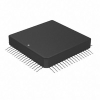
AD10242TZ Analog Devices Inc, AD10242TZ Datasheet - Page 12

AD10242TZ
Manufacturer Part Number
AD10242TZ
Description
IC,A/D CONVERTER,DUAL,12-BIT,HYBRID,QFP,68PIN
Manufacturer
Analog Devices Inc
Datasheet
1.AD10242BZ.pdf
(16 pages)
Specifications of AD10242TZ
Rohs Status
RoHS non-compliant
Number Of Bits
12
Sampling Rate (per Second)
40M
Data Interface
Parallel
Number Of Converters
2
Power Dissipation (max)
2W
Voltage Supply Source
Analog and Digital, Dual ±
Operating Temperature
-55°C ~ 125°C
Mounting Type
Surface Mount
Package / Case
68-CLCC
For Use With
AD10242/PCB - KIT EVAL PCB FOR AD10242
Lead Free Status / RoHS Status
Available stocks
Company
Part Number
Manufacturer
Quantity
Price
Part Number:
AD10242TZ
Manufacturer:
ADI/亚德诺
Quantity:
20 000
Company:
Part Number:
AD10242TZ/883
Manufacturer:
ZCOMM
Quantity:
1 400
AD10242
USING THE FLEXIBLE INPUT
The AD10242 has been designed with the user’s ease of opera-
tion in mind. Multiple input configurations have been included on
board to allow the user a choice of input signal levels and input
impedance. While the standard inputs are ± 0.5 V, ± 1.0 V, and
± 2.0 V, the user can select the input impedance of the AD10242
on any input by using the other inputs as alternate locations for
GND or an external resistor. The following chart summarizes the
impedance options available at each input location:
A
A
A
A
A
A
A
A
=
A
A
A
A
While the analog inputs of the AD10242 are designed for
dc- coupled bipolar inputs, the AD10242 has the ability to
use unipolar inputs in a user selectable mode through the addi-
tion of an external resistor. This allows for 1 V, 2 V, and 4 V
full-scale unipolar signals to be applied to the various inputs
(A
tor (typical, offset calibration required) between UPOS and
UCOM shifts the reference voltage setpoint to allow a unipolar
positive voltage to be applied at the inputs of the device. To cali-
brate offset, apply a midscale dc voltage to the converter while
adjusting the unipolar resistor for a midscale output transition.
To operate with –1 V, –2 V, or –4 V full-scale unipolar signals,
place a 2.67 kΩ resistor (typical, offset calibration required)
between UNEG and UCOM. This again shifts the reference volt-
age setpoint to allow a unipolar negative voltage to be applied at
the inputs of the device. To calibrate offset, apply a midscale dc
voltage to the converter while adjusting the unipolar resistor for
a midscale output transition.
IN
IN
IN
IN
IN
IN
IN
IN
IN
IN
IN
IN
IN
3 = 100 Ω when A
3 = 75 Ω when A
3 = 50 Ω when A
1 = 100 Ω when A
1 = 75 Ω when A
1 = 50 Ω when A
2 = 200 Ω when A
2 = 100 Ω when A
2 = 75 Ω when A
2 =
2 = 50 Ω when A
3 = 400 Ω.
1, A
300 Ω, with A
100 Ω, with A
IN
2, and A
Figure 13. Unipolar Positive
2.43k
IN
IN
IN
IN
IN
IN
IN
IN
3, respectively). Placing a 2.43 kΩ resis-
IN
IN
IN
IN
IN
3 is shorted to GND.
2 is shorted to GND.
2 to A
2 to A
3 has an external resistor of 92 Ω to GND.
3 has an external resistor of 57 Ω to GND.
3 has an external resistor of 133 Ω to GND.
3 shorted to GND.
3 shorted to GND.
2 and A
3 is open.
3 is shorted to GND.
IN
IN
A
A
A
UPOS
UCOM
IN
IN
IN
3 has an external resistor of
3 has an external resistor of
2
3
1
IN
3 are open.
AD10242
A
IN
2
–12–
GROUNDING AND DECOUPLING
Analog and Digital Grounding
Proper grounding is essential in any high speed, high resolution
system. Multilayer printed circuit boards (PCBs) are recom-
mended to provide optimal grounding and power schemes. The
use of ground and power planes offers distinct advantages:
1. The minimization of the loop area encompassed by a signal
2. The minimization of the impedance associated with ground
3. The inherent distributed capacitor formed by the power
These characteristics result in both a reduction of electro-
magnetic interference (EMI) and an overall improvement in
performance.
It is important to design a layout that prevents noise from cou-
pling to the input signal. Digital signals should not be run in
parallel with input signal traces and should be routed away from
the input circuitry. The AD10242 does not distinguish between
analog and digital ground pins as the AD10242 should always
be treated like an analog component. All ground pins should be
connected together directly under the AD10242. The PCB
should have a ground plane covering all unused portions of the
component side of the board to provide a low impedance path
and manage the power and ground currents. The ground plane
should be removed from the area near the input pins to reduce
stray capacitance.
LAYOUT INFORMATION
The schematic of the evaluation board (Figure 15) represents a
typical implementation of the AD10242. The pinout of the
AD10242 is very straightforward and facilitates ease of use
and the implementation of high frequency/high resolution
design practices. It is recommended that high quality ceramic
chip capacitors be used to decouple each supply pin to ground
directly at the device. All capacitors except the one placed on
ENCODE can be standard high quality ceramic chip capacitors.
The capacitor used on the ENCODE pin must be a low induc-
tance chip capacitor as referenced previously.
and its return path.
and power paths.
plane, PCB insulation, and ground plane.
Figure 14. Unipolar Negative
2.67k
A
A
A
UNEG
UCOM
IN
IN
IN
1
2
3
AD10242
REV. C


