AC164142 Microchip Technology, AC164142 Datasheet - Page 16
AC164142
Manufacturer Part Number
AC164142
Description
Consumer-band BPSK 7.2kbps PLM PICtail Plus Daughter Board Other
Manufacturer
Microchip Technology
Series
PICtail™ Plusr
Specifications of AC164142
Kit Application Type
Communication
Silicon Family Name
DsPIC
Kit Contents
2x Power-Line Soft-Modem PICtail Plus Daughter Boards, 2x High Voltage Adapter Cables, Info Sheet
Features
Operates On 5V And 9V
Rohs Compliant
Yes
Processor To Be Evaluated
dsPIC33F
Processor Series
dsPIC33F
Operating Supply Voltage
5 V, 9 V
Featured Product
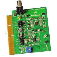
AC164142 PICtail⢠Plus Daughter Board
Main Purpose
Interface, Power Line Transceiver
Embedded
No
Utilized Ic / Part
-
Primary Attributes
AC Power Line Transceiver, BPSK 7.2 Kbps
Secondary Attributes
Requires Explorer 16 Boards
Lead Free Status / Rohs Status
Lead free / RoHS Compliant
Available stocks
Company
Part Number
Manufacturer
Quantity
Price
Company:

Part Number:
AC164142
Manufacturer:
MICROCHIP
Quantity:
12 000
Part Number:
AC164142
Manufacturer:
BOARD
Quantity:
20 000


Consumer-band BPSK 7.2 kbps PLM PICtail™ Plus Daughter Board User’s Guide
DS70656A-page 16
2.1.1
The daughter board utilizes four PWM channels to generate an approximated sine
wave. The PWM channels are shifted in phase such that a sum of their instantaneous
amplitude resembles a stepped sine wave. By filtering this stepped sine wave using a
band-pass filter, a relatively clean sine wave is obtained, as shown in
amount of filtering required is dependent on the number of PWM channels. Using
higher number of PWM channels will require less filtering.
FIGURE 2-2:
After the approximated sine wave is obtained, it is amplified by the MCP6283 Op amp.
The Chip Select pin of this Op amp is used to implement flow-control. By asserting the
HiZ pin, the transmit amplifier is enabled, thus enabling the transmission path. This HiZ
pin can be configured on RG0/ RG1/RF0/RF1 using the jumper, JP2.
The output of this transmit amplifier is fed to the line driver circuit implemented using
transistors in a push-pull configuration. The line driver output is then coupled into the
power line through the HV adapter cable.
2.1.2
The modulated signal on the power line is received by the HV adapter cable and is
passed through an LC band-pass filter to filter out the noise and interference. This fil-
tered signal is then fed to the tuned amplifier, which is implemented using a transistor
amplifier in a common-emitter configuration. This amplified signal is then filtered using
a high-gain 2-stage active band-pass filter designed around the MCP6282 Op amp.
The output of this filter is then fed to the Analog-to-Digital Converter (ADC) input of the
dsPIC33F DSC device on the Explorer 16 Development Board. The ADC input pins,
AN8/AN9/AN16/AN17, can be selected by appropriately setting the jumper, JP3.
Band-pass
Output
PWM1
PWM2
PWM3
PWM4
Filter
Transmit Path
Receive Path
PWM-BASED ANALOG SIGNAL GENERATION
© 2011 Microchip Technology Inc.
Figure
2-2. The
Related parts for AC164142
Image
Part Number
Description
Manufacturer
Datasheet
Request
R

Part Number:
Description:
Manufacturer:
Microchip Technology Inc.
Datasheet:
Part Number:
Description:
Manufacturer:
Microchip Technology Inc.
Datasheet:
Part Number:
Description:
Manufacturer:
Microchip Technology Inc.
Datasheet:
Part Number:
Description:
Manufacturer:
Microchip Technology Inc.
Datasheet:
Part Number:
Description:
Manufacturer:
Microchip Technology Inc.
Datasheet:
Part Number:
Description:
Manufacturer:
Microchip Technology Inc.
Datasheet:
Part Number:
Description:
Manufacturer:
Microchip Technology Inc.
Datasheet:
Part Number:
Description:
Manufacturer:
Microchip Technology Inc.
Datasheet: