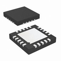
AD7298-1BCPZ Analog Devices Inc, AD7298-1BCPZ Datasheet - Page 4

AD7298-1BCPZ
Manufacturer Part Number
AD7298-1BCPZ
Description
8Channel 10Bit SAR
Manufacturer
Analog Devices Inc
Datasheet
1.AD7298-1BCPZ.pdf
(24 pages)
Specifications of AD7298-1BCPZ
Number Of Bits
10
Sampling Rate (per Second)
1M
Data Interface
Serial, SPI™
Number Of Converters
1
Power Dissipation (max)
23mW
Voltage Supply Source
Single Supply
Operating Temperature
-40°C ~ 125°C
Mounting Type
Surface Mount
Package / Case
20-WFQFN, CSP Exposed Pad
Resolution (bits)
10bit
Sampling Rate
1MSPS
Input Channel Type
Single Ended
Supply Voltage Range - Analog
1.65V To 3.6V
Digital Ic Case Style
LFCSP
Rohs Compliant
Yes
Lead Free Status / RoHS Status
Lead free / RoHS Compliant
Available stocks
Company
Part Number
Manufacturer
Quantity
Price
Company:
Part Number:
AD7298-1BCPZ
Manufacturer:
ADI
Quantity:
200
AD7298-1
Parameter
LOGIC OUTPUTS
CONVERSION RATE
POWER REQUIREMENTS
1
2
3
4
5
6
All specifications expressed in decibels are referred to full-scale input FSR and tested with an input signal at 0.5 dB below full scale, unless otherwise specified.
See the Terminology section.
Sample tested during initial release to ensure compliance.
Refers to the
I
Power dissipation is specified with V
TOTAL
Output High Voltage, V
Output Low Voltage, V
Floating State Leakage Current
Floating State Output Capacitance
Conversion Time
Track-and-Hold Acquisition Time
Throughput Rate
V
V
I
Power Dissipation
TOTAL
DD
DRIVE
Normal Mode (Operational)
Normal Mode (Static)
Partial Power-Down Mode
Full Power-Down Mode
Normal Mode (Operational)
Normal Mode (Static)
Partial Power-Down Mode
Full Power-Down Mode
is the total current flowing in V
5
V
REF
p
in specified for 25°C.
6
OL
OH
DD
DD
and V
= V
2, 3
DRIVE
3
DRIVE
= 3.6 V, unless otherwise noted.
.
Min
V
V
2.8
1.65
DRIVE
DRIVE
− 0.3
− 0.2
Rev. A | Page 4 of 24
Typ
±0.01
8
1
3
3
5.8
4.1
2.7
1
17.4
14.8
9.8
3.6
Max
0.4
±1
t
100
1
3.6
3.6
6.4
4.6
3.3
1.6
10
19.2
23
16.6
11.9
5.8
36
2
+ (16 × t
SCLK
)
Unit
V
V
V
μA
pF
μs
ns
MSPS
V
V
mA
mA
mA
μA
μA
mW
mW
mW
mW
μW
μW
Test Conditions/Comments
V
V
For V
Full-scale step input
f
conversions, one cycle latency
Digital inputs = 0 V or V
V
T
T
V
T
T
SCLK
A
A
A
A
DRIVE
DRIVE
DD
DD
= −40°C to +25°C
= −40°C to +125°C
= −40°C to +25°C
= −40°C to +125°C
= 3.6 V, V
= 3 V, V
= 20 MHz; for analog voltage
IN0
< 1.8
≥ 1.8
to V
DRIVE
IN7
DRIVE
with one cycle latency
= 3 V
= 3.6 V
DRIVE


