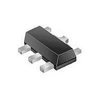
NCP4641H080T1G ON Semiconductor, NCP4641H080T1G Datasheet

NCP4641H080T1G
Specifications of NCP4641H080T1G
Available stocks
Related parts for NCP4641H080T1G
NCP4641H080T1G Summary of contents
Page 1
NCP4641 150 mA, Wide Input Range, Voltage Regulator The NCP4641 is a CMOS 150 mA linear voltage regulator with high input voltage and ultra−low supply current. It incorporates multiple protection features such as peak current limit, short circuit current limit ...
Page 2
VIN CE Figure 2. Simplified Schematic Block Diagram PIN FUNCTION DESCRIPTION Pin No. Pin No. SOT89 SOIC6− − Internal VR Vref Current Limit Short Protection Thermal Shutdown Pin Name ...
Page 3
ABSOLUTE MAXIMUM RATINGS Rating Input Voltage Peak Input Voltage (Note 1) Output Voltage Chip Enable Input Output Current Power Dissipation SOT−89 Power Dissipation SOIC6−TL Junction Temperature Storage Temperature ESD Capability, Human Body Model (Note 2) ESD Capability, Machine Model (Note ...
Page 4
ELECTRICAL CHARACTERISTICS Parameter Operating Input Voltage Output Voltage Output Voltage Temp. Coeffi cient Line Regulation V IN Load Regulation OUT Dropout Voltage I OUT Output Current V IN Short ...
Page 5
5.5 V 2.5 2.0 1.5 1.0 0.5 0 100 150 200 I (mA) OUT Figure 3. Output Voltage vs. Output Current 3.0 V Version ( 5C) J 9.0 8.0 ...
Page 6
T , JUNCTION TEMPERATURE (°C) J Figure 9. Output Voltage vs. Temperature, 3.0 V Version 8.10 8.08 8.06 8.04 8.02 8.00 7.98 7.96 7.94 ...
Page 7
OUT 1.0 0 INPUT VOLTAGE (V) IN Figure 15. Output Voltage vs. Input Voltage, 5.0 V Version 100 90 80 ...
Page 8
FREQUENCY (kHz) Figure 21. Output Voltage Noise, 5.0 V Version 8 OUT 4.50 4.00 3.50 3.00 2.50 2.00 0 0.2 Figure 23. ...
Page 9
TYPICAL CHARACTERISTICS 9.00 8.50 8.00 7.50 7.00 6.50 0 0.2 0.4 0.6 0.8 1.0 1.2 t (ms) Figure 25. Line Transients, 8.0 V Version ms OUT 1.24 1.22 1.20 ...
Page 10
TYPICAL CHARACTERISTICS 5.05 5.03 5.01 4.99 4.97 4. 100 120 140 160 180 200 t (ms) Figure 28. Load Transients, 8.0 V Version – ms, ...
Page 11
TYPICAL CHARACTERISTICS Chip Enable OUT OUT I = 150 mA OUT 2 0 − 100 150 200 250 300 350 400 450 500 t (ms) Figure 31. ...
Page 12
... Device NCP4641H030T1G 3.0 V NCP4641H050T1G 5.0 V NCP4641H080T1G 8.0 V †For information on tape and reel specifications, including part orientation and tape sizes, please refer to our Tape and Reel Packaging Specifications Brochure, BRD8011/D. *To order other package and voltage variants, please contact your ON Semiconductor sales representative. ...
Page 13
... SEATING PLANE *For additional information on our Pb−Free strategy and soldering details, please download the ON Semiconductor Soldering and Mounting Techniques Reference Manual, SOLDERRM/D. PACKAGE DIMENSIONS SOIC6 (HSOP6) CASE 751BR−01 ISSUE O NOTES SEATING C PLANE DETAIL A D DETAIL A RECOMMENDED SOLDERING FOOTPRINT* 3.81 ...
Page 14
... Pb−Free strategy and soldering details, please download the ON Semiconductor Soldering and Mounting Techniques Reference Manual, SOLDERRM/D. N. American Technical Support: 800−282−9855 Toll Free USA/Canada Europe, Middle East and Africa Technical Support: Phone: 421 33 790 2910 Japan Customer Focus Center Phone: 81− ...


