MM3Z5V1ST1 ON Semiconductor, MM3Z5V1ST1 Datasheet

DIODE ZENER 5.1V 200MW SOD-323

MM3Z5V1ST1

Manufacturer Part Number
MM3Z5V1ST1
Description
DIODE ZENER 5.1V 200MW SOD-323
Manufacturer
ON Semiconductor
Datasheet

Specifications of MM3Z5V1ST1

Voltage - Zener (nom) (vz)
5.1V
Voltage - Forward (vf) (max) @ If
900mV @ 10mA
Current - Reverse Leakage @ Vr
2µA @ 2V
Power - Max
200mW
Impedance (max) (zzt)
60 Ohm
Mounting Type
Surface Mount
Package / Case
SC-76, SOD-323, UMD2
Operating Temperature
-65°C ~ 150°C
Lead Free Status / RoHS Status
Contains lead / RoHS non-compliant
Tolerance
-
Other names
MM3Z5V1ST1OS
MM3Z5V1ST1OS
MM3Z5V1ST1OSTR

Available stocks

Company
Part Number
Manufacturer
Quantity
Price
Part Number:
MM3Z5V1ST1G
Quantity:
411 000
Part Number:
MM3Z5V1ST1G
Manufacturer:
ON
Quantity:
30 000
Part Number:
MM3Z5V1ST1G
Manufacturer:
ON/安森美
Quantity:
20 000
Part Number:
MM3Z5V1ST1G
0
Company:
Part Number:
MM3Z5V1ST1G
Quantity:
39 000
MM3Z2V4ST1 SERIES
Zener Voltage Regulators
200 mW SOD−323 Surface Mount
Tight Tolerance Portfolio
mount package that has a power dissipation of 200 mW. They are
designed to provide voltage regulation protection and are especially
attractive in situations where space is at a premium. They are well
suited for applications such as cellular phones, hand−held portables,
and high density PC boards.
Specification Features:
Mechanical Characteristics:
CASE:
FINISH:
MAXIMUM CASE TEMPERATURE FOR SOLDERING PURPOSES:
LEADS:
POLARITY:
FLAMMABILITY RATING:
MOUNTING POSITION:
Maximum ratings are those values beyond which device damage can occur.
Maximum ratings applied to the device are individual stress limit values (not
normal operating conditions) and are not valid simultaneously. If these limits are
exceeded, device functional operation is not implied, damage may occur and
reliability may be affected.
1. FR−4 Minimum Pad
MAXIMUM RATINGS
July, 2004 − Rev. 9
Total Device Dissipation FR−5 Board,
Thermal Resistance from
Junction and Storage
Temperature Range
This series of Zener diodes is packaged in a SOD−323 surface
260 C for 10 Seconds
Low Body Height: 0.035 (0.9 mm)
Standard Zener Breakdown Voltage Range −
Steady State Power Rating of 200 mW
Small Body Outline Dimensions:
Package Weight: 4.507 mg/unit
ESD Rating of Class 3 (>16 kV) per Human Body Model
Tight Tolerance V
Pb−Free Packages are Available
Semiconductor Components Industries, LLC, 2004
Void-free, transfer-molded plastic
All external surfaces are corrosion resistant
Plated with Pb−Sn or Sn only (Pb−Free)
(Note 1) @ T
Derate above 25 C
Junction−to−Ambient
2.4 V to 12 V
0.067 x 0.049 (1.7 mm x 1.25 mm)
Cathode indicated by polarity band
Rating
Z
A
= 25 C
Any
UL 94 V−0
Symbol
T
R
J
P
, T
qJA
D
stg
−65 to +150
Max
200
635
1.5
1
mW/ C
Unit
mW
C/W
C
†For information on tape and reel specifications,
See specific marking information in the device marking
column of the Electrical Characteristics table on page 2 of
this data sheet.
MM3ZxxxST1
MM3ZxxxST3
MM3ZxxxST1G
MM3ZxxxST3G
including part orientation and tape sizes, please
refer to our Tape and Reel Packaging Specifications
Brochure, BRD8011/D.
Device
1
CASE 477
DEVICE MARKING INFORMATION
SOD−323
STYLE 1
ORDERING INFORMATION
Cathode
1
http://onsemi.com
2
(Pb−Free)
(Pb−Free)
SOD−323
SOD−323
SOD−323
SOD−323
Package
xx = Specific Device Code
M = Date Code
Publication Order Number:
MARKING
DIAGRAM
10,000/Tape & Reel
10,000/Tape & Reel
3000/Tape & Reel
3000/Tape & Reel
Anode
MM3Z2V4ST1/D
2
Shipping
xx M

Related parts for MM3Z5V1ST1

MM3Z5V1ST1 Summary of contents

Page 1

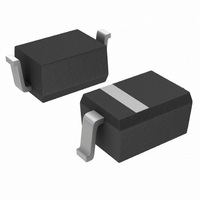
MM3Z2V4ST1 SERIES Zener Voltage Regulators 200 mW SOD−323 Surface Mount Tight Tolerance Portfolio This series of Zener diodes is packaged in a SOD−323 surface mount package that has a power dissipation of 200 mW. They are designed to provide voltage ...

Page 2

... Device Current Marking Izt mA Device MM3Z2V4ST1 T2 5.0 MM3Z2V7ST1 T3 5.0 MM3Z3V3ST1 T5 5.0 MM3Z3V3TT1 5.0 MM3Z3V6ST1 5.0 MM3Z3V9ST1 5.0 MM3Z4V3ST1 T8 5.0 MM3Z4V7ST1 5.0 MM3Z5V1ST1 TA 5.0 MM3Z5V6ST1 TC 5.0 MM3Z6V2ST1 TE 5.0 MM3Z6V8ST1 TF 5.0 MM3Z7V5ST1 TG 5.0 MM3Z8V2ST1 TH 5.0 MM3Z9V1ST1 TK 5.0 MM3Z10VST1 WB 5.0 MM3Z11VST1 WC 5.0 MM3Z12VST1 TN 5.0 ...

Page 3

Z(AC kHz 100 1.0 3 NOMINAL ZENER VOLTAGE Z Figure 1. Effect of Zener Voltage on Zener Impedance 1000 1 V BIAS 0 V BIAS ...

Page 4

... NOTE 5 NOTE 3 *For additional information on our Pb−Free strategy and soldering details, please download the ON Semiconductor Soldering and Mounting Techniques Reference Manual, SOLDERRM/D. ON Semiconductor and are registered trademarks of Semiconductor Components Industries, LLC (SCILLC). SCILLC reserves the right to make changes without further notice to any products herein ...

Related keywords